Advanced 3D Packaging Market Size, Share, Growth Opportunity Analysis Report by Packaging Technology 3D Through-Silicon Via 3D TSV, 3D Fan-Out (3D FO), 3D Wafer-Level Chip-Scale Packaging (3D WLCSP), 3D Interposer-Based Packaging, 3D Stacked Die Packaging, Hybrid Bonding-Based 3D Packaging, and Others), Material Type, Interconnection Type, Device Application, Node Size, Component Integration, End-user Industry, and Geography (North America, Europe, Asia Pacific, Middle East, Africa, and South America) – Global Industry Data, Trends, and Forecasts, 2025–2035
|
Market Structure & Evolution |
|
|
Segmental Data Insights |
|
|
Demand Trends |
|
|
Competitive Landscape |
|
|
Strategic Development |
|
|
Future Outlook & Opportunities |
|
Advanced 3D Packaging Market Size, Share, and Growth
The global advanced 3D packaging market is projected to grow from USD 7.9 Billion in 2025 to USD 28.4 Billion by 2035, with a strong CAGR of 12.3% during the forecast period. The growth is driven by the proliferation of chip miniaturization, heterogeneous integration, and high-performance computing in consumer electronics, automotive, and cloud infrastructure

Broadcom launched its pioneering 3.5D eXtreme Dimension System‑in‑Package (XDSiP) platform, which integrates up to 12 HBM memory stacks and over 6000 mm² of silicon into a single package. This face‑to‑face (F2F) packaging technology delivers exceptional interconnect density, reduced latency, and notably higher power efficiency, ushering in a new era for AI, high-performance computing, and next-gen semiconductor design.
Innovation is also helping the market growth. For instance, TSMC initiated mass production of its 3DFabric platform, which uses CoWoS and InFO technologies to power complex AI chips with significantly improved memory bandwidth and interconnect efficiency.
These advances are enabling semiconductor companies to produce faster, smaller and more power-efficient chips to meet surging demand in areas such as machine learning, autonomous driving and next-gen networking. With applications increasing in data intensity, the advanced 3D packaging market is ready to serve as a key enabler for performance, cost, and integration in the worldwide chip industry.

Advanced 3D Packaging Market Dynamics and Trends
Driver: Expansion of advanced packaging capacity amid global semiconductor reshoring
- The trend toward localized semiconductor manufacturing has accelerated investment in advanced 3D-packaging infrastructure. For instance, in 2024, Samsung, announced huge investment plans in Texas, originally DEC have $17 billion and later expanding to over $40 billion investment under CHIPS in the SCIENCE act, for a new semiconductor site in Taylor with an advanced packaging plant that is to be world leading.
- This will not only enhance the regional capacity for chip manufacturing and packaging, but will pursue the domestic manufacture of two‑nanometre and four‑nanometre chips. The expansion also will further strengthen supply chain resiliency and establish national leadership in AI‑driven chips, while creating thousands of high‑tech jobs.
Restraint: High Cost and Complexity of Advanced Packaging Infrastructure
- Despite the increasing demand for high-performance and low-profile semiconductor packaging, the cost of investment and operation in high-end 3D packaging factories is a major challenge, particularly as thermal management, insulation materials, and interface reliability supported by PTFE tapes and films which become more critical at advanced nodes. For instance, Intel’s advanced packaging plant Bio Valley, required billions in capital expenditure, reflecting high bar to entry for scalable operations.
- Additional challenges of technical nature including thermal issues, yield production and interconnect reliability. A single failing die or interposer in the stack can make an entire stack mutually unusable, resulting in costly production waste. These problems underpin the fact that advanced 3D packaging market is to ramp effectively, innovations in cost-effective integration methods and improved process yield are essential especially as demand extends beyond Tier 1 players.
Opportunity: Growth in Food Safety and Healthcare Applications
- Advanced 3D packaging is enabling new uses in AI, autonomous vehicles and implantable medical devices that need high-performance computing power in tight quarters, strengthening requirements for reliability, miniaturization, and integration in medical device packaging. These applications require higher chip density, faster interconnects, and lower latency that only heterogeneous 3D integration and system-in-package (SiP) solutions can provide. For Instance, in 2023, AMD utilized 3D chiplet technology on its EPYC Genoa-X processors featuring stacked L3 cache, resulting in a dramatic performance uplift in data analytics and cloud AI workloads.
- In the medical field, miniaturized implantable devices and wearable medical instruments are more and more depended on chip stack and hybrid bond to meet the terrain and function in a small area. Taking things further for chronic care, 3D packaging is now enabling companies such as Abbott and Medtronic to place sensors, memory, and processors in a tiny footprint, pushing edge diagnostics and real-time monitoring for application in chronic care. This cross-industry demand is driving ongoing demand and innovation around advanced 3D packaging solutions.
Key Trend: Rise of Open Standards and Novel Chiplet Ecosystems
- The semiconductor industry is quickly adopting open interfaces and chiplet-based design, where several firms can contribute parts into monolithic packages. The change accelerates innovation, increases interoperability, and reduces time to market by providing a way to mix and match heterogeneous dies from various vendors and build them into a single 3D package. this movement enables Universal Chiplet Interconnect Express (UCIe) standard.
- For instance, the UCIe Consortium published version 2.0 in August 2024, its interface evolved by introducing support for advanced features like runtime monitoring, debugging, and 3D packaging while preserving backward compatibility with previous versions. UCIe’s adoption sets the scene for chiplet integration to be commercialized widely, allows small players to leverage leading-edge technologies and is helping the broader advanced 3D packaging market to scale rapidly.
Advanced 3D Packaging Market Analysis and Segmental Data

3D Through-Silicon Via (3D TSV) Technology holds majority share in Advanced 3D Packaging Market
- 3D Through-Silicon Via (3D TSV) technology holds ~35% share in the advanced 3D packaging market, owing to its high-density vertical interconnects that drastically improve performance, reduce footprint, and lower power consumption. This is ideal for high-bandwidth applications, including data centres, AI processors and high-performance memory stacks. For instance, Samsung’s HBM3 memory, which utilized 3D TSV for stacking DRAM dies, reached bandwidth exceeding 800 GB/s in 2023 for high-performance AI and HPC workloads.
- These developments optimize gain bandwidth, speed, thermal performance, and design flexibility which are also vital in the scaling of next-generation computing. Fan-out and hybrid bonding are emerging in niche markets, but 3D TSV is the main and well-established technology going into commercial volume production, because of its reliability and simplicity, anticipated to further driving for market leadership during the forecast preriod.
Asia Pacific Dominates Advanced 3D Packaging in 2025 and Beyond
- Asia Pacific is the largest regional market holding the share of 53.4%, driven by early adoption of advanced 3D packaging, strong semiconductor manufacturing bases in countries like Taiwan, South Korea, China, and Japan. Leading companies in the region like TSMC, Samsung, ASE Group among others, are investing heavily in advanced packaging, fan-out wafer-level packaging and hybrid bonding, to address growing global demand from the AI, automotive and consumer electronics segments.
- Government-supported policies for semiconductors and regional reshoring initiatives are consolidating Asia Pacific’s lead. For Instance, China’s “Made in China 2025” and Korea’s $450 billion semiconductor investment plan will boost local packaging infrastructure. Meanwhile, foundries and OSAT suppliers partner to enable the ecosystem to mature. Asia Pacific will dominate the market over the research period, with high output production, skilled labour and strong supply chains.
Advanced 3D Packaging Market Ecosystem
The global Advanced 3D Packaging market exhibits a highly consolidated structure, driven by the presence of dominant Tier 1 players such as TSMC, Intel, and Samsung Electronics, alongside Tier 2 firms like ASE Technology Group, Amkor Technology, and JCET Group, and emerging Tier 3 contributors. Tier 1 players exert high influence over technological roadmaps and capacity control. Porter’s Five Forces reveals high supplier concentration due to limited advanced node packaging capabilities, while buyer concentration remains moderate, as demand is dispersed across major semiconductor and electronics firms.

Recent Developments and Strategic Overview
- In April 2025, TSMC announced plans to construct two major advanced packaging fabs next to existing fabs in Arizona, production capacity commitment prior to its six-fab roadmap. This extension to TSMC’s 3D Fabric offerings is to address the increasing demand for chip-on-wafer-on-substrate (CoWoS) and other 3D packaging technology for domestic AI and datacenter customers, and to diminish global supply chain risks.
- In January 2024, Intel announced its Fab 9 had begun operations at its Rio Rancho site in New Mexico. The $3.5 billion production facility was built to package chips using Foveros 3D technology and is one of Intel's first fabs dedicated solely to advanced packaging technologies.
Report Scope
|
Attribute |
Detail |
|
Market Size in 2025 |
USD 7.9 Billion |
|
Market Forecast Value in 2035 |
USD 24.8 Billion |
|
Growth Rate (CAGR) |
12.3% |
|
Forecast Period |
2025 – 2035 |
|
Historical Data Available for |
2021 – 2024 |
|
Market Size Units |
US$ Billion for Value |
|
Report Format |
Electronic (PDF) + Excel |
|
Regions and Countries Covered |
|||||
|
North America |
Europe |
Asia Pacific |
Middle East |
Africa |
South America |
|
|
|
|
|
|
|
Companies Covered |
|||||
|
|
|
|
|
|
Advanced 3D Packaging Market Segmentation and Highlights
|
Segment |
Sub-segment |
|
By Packaging |
|
|
By Material
|
|
|
By Interconnection
|
|
|
By Device Type |
|
|
By Node Size
|
|
|
By Component |
|
|
By End-User Industry |
|
Frequently Asked Questions
Table of Contents
- 1. Research Methodology and Assumptions
- 1.1. Definitions
- 1.2. Research Design and Approach
- 1.3. Data Collection Methods
- 1.4. Base Estimates and Calculations
- 1.5. Forecasting Models
- 1.5.1. Key Forecast Factors & Impact Analysis
- 1.6. Secondary Research
- 1.6.1. Open Sources
- 1.6.2. Paid Databases
- 1.6.3. Associations
- 1.7. Primary Research
- 1.7.1. Primary Sources
- 1.7.2. Primary Interviews with Stakeholders across Ecosystem
- 2. Executive Summary
- 2.1. Advanced 3D Packaging Market Outlook
- 2.1.1. Advanced 3D Packaging Market Size in Value (US$ Billion), and Forecasts, 2021-2035
- 2.1.2. Compounded Annual Growth Rate Analysis
- 2.1.3. Growth Opportunity Analysis
- 2.1.4. Segmental Share Analysis
- 2.1.5. Geographical Share Analysis
- 2.2. Market Analysis and Facts
- 2.3. Supply-Demand Analysis
- 2.4. Competitive Benchmarking
- 2.5. Go-to- Market Strategy
- 2.5.1. Customer/ End-use Industry Assessment
- 2.5.2. Growth Opportunity Data, 2025-2035
- 2.5.2.1. Regional Data
- 2.5.2.2. Country Data
- 2.5.2.3. Segmental Data
- 2.5.3. Identification of Potential Market Spaces
- 2.5.4. GAP Analysis
- 2.5.5. Potential Attractive Price Points
- 2.5.6. Prevailing Market Risks & Challenges
- 2.5.7. Preferred Sales & Marketing Strategies
- 2.5.8. Key Recommendations and Analysis
- 2.5.9. A Way Forward
- 2.1. Advanced 3D Packaging Market Outlook
- 3. Industry Data and Premium Insights
- 3.1. Global Industry Overview, 2025
- 3.1.1. Industry Ecosystem Analysis
- 3.1.2. Key Trends for Electronics & Semiconductors Industry
- 3.1.3. Regional Distribution for Industry
- 3.2. Supplier Customer Data
- 3.3. Source Roadmap and Developments
- 3.4. Trade Analysis
- 3.4.1. Import & Export Analysis, 2025
- 3.4.2. Top Importing Countries
- 3.4.3. Top Exporting Countries
- 3.5. Trump Tariff Impact Analysis
- 3.5.1. Manufacturer
- 3.5.2. Supply Chain/Distributor
- 3.5.3. End Consumer
- 3.1. Global Industry Overview, 2025
- 4. Market Overview
- 4.1. Market Dynamics
- 4.1.1. Drivers
- 4.1.1.1. Rising demand for miniaturized electronic devices across consumer electronics, including wearables, AR/VR, and smartphones.
- 4.1.1.2. Increasing focus on power efficiency and thermal performance in semiconductor devices to support AI, gaming, and cloud workloads.
- 4.1.1.3. Collaboration between foundries and OSAT players to develop cost-effective, scalable 3D packaging solutions.
- 4.1.2. Restraints
- 4.1.2.1. High capital investment required for infrastructure, equipment, and R&D limits adoption by small and mid-tier semiconductor companies.
- 4.1.2.2. Technical challenges in yield management and interconnect reliability, especially in complex multi-die configurations.
- 4.1.1. Drivers
- 4.2. Key Trend Analysis
- 4.3. Regulatory Framework
- 4.3.1. Key Regulations, Norms, and Subsidies, by Key Countries
- 4.3.2. Tariffs and Standards
- 4.3.3. Impact Analysis of Regulations on the Market
- 4.4. Value Chain Analysis
- 4.4.1. Material/ Component
- 4.4.2. Foundries and IDMs
- 4.4.3. OSATs
- 4.4.4. System Integrators
- 4.4.5. End-users/ Customers
- 4.5. Raw Material Analysis
- 4.6. Cost Structure Analysis
- 4.6.1. Parameter’s Share for Cost Associated
- 4.6.2. COGP vs COGS
- 4.6.3. Profit Margin Analysis
- 4.7. Pricing Analysis
- 4.7.1. Regional Pricing Analysis
- 4.7.2. Segmental Pricing Trends
- 4.7.3. Factors Influencing Pricing
- 4.8. Porter’s Five Forces Analysis
- 4.9. PESTEL Analysis
- 4.10. Advanced 3D Packaging Market Demand
- 4.10.1. Historical Market Size - in Value (US$ Billion), 2021-2024
- 4.10.2. Current and Future Market Size - in Value (US$ Billion), 2025–2035
- 4.10.2.1. Y-o-Y Growth Trends
- 4.10.2.2. Absolute $ Opportunity Assessment
- 4.1. Market Dynamics
- 5. Competition Landscape
- 5.1. Competition structure
- 5.1.1. Fragmented v/s consolidated
- 5.2. Company Share Analysis, 2025
- 5.2.1. Global Company Market Share
- 5.2.2. By Region
- 5.2.2.1. North America
- 5.2.2.2. Europe
- 5.2.2.3. Asia Pacific
- 5.2.2.4. Middle East
- 5.2.2.5. Africa
- 5.2.2.6. South America
- 5.3. Product Comparison Matrix
- 5.3.1. Specifications
- 5.3.2. Market Positioning
- 5.3.3. Pricing
- 5.1. Competition structure
- 6. Advanced 3D Packaging Market Analysis, by Packaging Technology
- 6.1. Key Segment Analysis
- 6.2. Advanced 3D Packaging Market Size in Value (US$ Billion), Analysis, and Forecasts, by Packaging Technology, 2021-2035
- 6.2.1. 3D Through-Silicon Via (3D TSV)
- 6.2.2. 3D Fan-Out (3D FO)
- 6.2.3. 3D Wafer-Level Chip-Scale Packaging (3D WLCSP)
- 6.2.4. 3D Interposer-Based Packaging
- 6.2.5. 3D Stacked Die Packaging
- 6.2.6. Hybrid Bonding-Based 3D Packaging
- 6.2.7. Others
- 7. Advanced 3D Packaging Market Analysis, by Material Type
- 7.1. Key Segment Analysis
- 7.2. Advanced 3D Packaging Market Size in Value (US$ Billion), Analysis, and Forecasts, by Material Type, 2021-2035
- 7.2.1. Substrates
- 7.2.2. Interposers (Silicon, Glass, Organic)
- 7.2.3. Dielectric Materials
- 7.2.4. Underfill Materials
- 7.2.5. Adhesives & Encapsulation Materials
- 7.2.6. Solders and Bumps
- 7.2.7. Others
- 8. Advanced 3D Packaging Market Analysis, by Interconnection Type
- 8.1. Key Segment Analysis
- 8.2. Advanced 3D Packaging Market Size in Value (US$ Billion), Analysis, and Forecasts, by Interconnection Type, 2021-2035
- 8.2.1. Through-Silicon Via (TSV)
- 8.2.2. Micro-Bumps
- 8.2.3. Hybrid Bonding
- 8.2.4. Wire Bonding
- 8.2.5. Copper Pillar Bumping
- 8.2.6. Others
- 9. Advanced 3D Packaging Market Analysis, by Device Application
- 9.1. Key Segment Analysis
- 9.2. Advanced 3D Packaging Market Size in Value (US$ Billion), Analysis, and Forecasts, by Device Application, 2021-2035
- 9.2.1. Memory Devices
- 9.2.2. Logic Devices
- 9.2.3. Image Sensors
- 9.2.4. LEDs
- 9.2.5. RF Devices
- 9.2.6. Power Devices
- 9.2.7. Others
- 10. Advanced 3D Packaging Market Analysis, by Node Size
- 10.1. Key Segment Analysis
- 10.2. Advanced 3D Packaging Market Size in Value (US$ Billion), Analysis, and Forecasts, by Node Size, 2021-2035
- 10.2.1. 7 nm and Below
- 10.2.2. 8–16 nm
- 10.2.3. 17–28 nm
- 10.2.4. 28 nm and Above
- 11. Advanced 3D Packaging Market Analysis, by Component Integration
- 11.1. Key Segment Analysis
- 11.2. Advanced 3D Packaging Market Size in Value (US$ Billion), Analysis, and Forecasts, by Component Integration, 2021-2035
- 11.2.1. System-in-Package (SiP)
- 11.2.2. Heterogeneous Integration
- 11.2.3. Monolithic 3D ICs
- 11.2.4. Others
- 12. Advanced 3D Packaging Market Analysis, by End-User Industry
- 12.1. Key Segment Analysis
- 12.2. Advanced 3D Packaging Market Size in Value (US$ Billion), Analysis, and Forecasts, by End-User Industry, 2021-2035
- 12.2.1. Consumer Electronics
- 12.2.2. Telecommunication
- 12.2.3. Automotive & Transportation
- 12.2.4. Healthcare/Medical Devices
- 12.2.5. Aerospace & Defense
- 12.2.6. Industrial Equipment
- 12.2.7. Others
- 13. Advanced 3D Packaging Market Analysis and Forecasts, by Region
- 13.1. Key Findings
- 13.2. Advanced 3D Packaging Market Size in Value (US$ Billion), Analysis, and Forecasts, by Region, 2021-2035
- 13.2.1. North America
- 13.2.2. Europe
- 13.2.3. Asia Pacific
- 13.2.4. Middle East
- 13.2.5. Africa
- 13.2.6. South America
- 14. North America Advanced 3D Packaging Market Analysis
- 14.1. Key Segment Analysis
- 14.2. Regional Snapshot
- 14.3. North America Advanced 3D Packaging Market Size in Value (US$ Billion), Analysis, and Forecasts, 2021-2035
- 14.3.1. Packaging Technology
- 14.3.2. Material Type
- 14.3.3. Interconnection Type
- 14.3.4. Device Application
- 14.3.5. Node Size
- 14.3.6. Component Integration
- 14.3.7. End-User Industry
- 14.3.8. Country
-
- 14.3.8.1.1. USA
- 14.3.8.1.2. Canada
- 14.3.8.1.3. Mexico
-
- 14.4. USA Advanced 3D Packaging Market
- 14.4.1. Country Segmental Analysis
- 14.4.2. Packaging Technology
- 14.4.3. Material Type
- 14.4.4. Interconnection Type
- 14.4.5. Device Application
- 14.4.6. Node Size
- 14.4.7. Component Integration
- 14.4.8. End-User Industry
- 14.5. Canada Advanced 3D Packaging Market
- 14.5.1. Country Segmental Analysis
- 14.5.2. Packaging Technology
- 14.5.3. Material Type
- 14.5.4. Interconnection Type
- 14.5.5. Device Application
- 14.5.6. Node Size
- 14.5.7. Component Integration
- 14.5.8. End-User Industry
- 14.6. Mexico Advanced 3D Packaging Market
- 14.6.1. Country Segmental Analysis
- 14.6.2. Packaging Technology
- 14.6.3. Material Type
- 14.6.4. Interconnection Type
- 14.6.5. Device Application
- 14.6.6. Node Size
- 14.6.7. Component Integration
- 14.6.8. End-User Industry
- 15. Europe Advanced 3D Packaging Market Analysis
- 15.1. Key Segment Analysis
- 15.2. Regional Snapshot
- 15.3. Europe Advanced 3D Packaging Market Size in Value (US$ Billion), Analysis, and Forecasts, 2021-2035
- 15.3.1. Country Segmental Analysis
- 15.3.2. Packaging Technology
- 15.3.3. Material Type
- 15.3.4. Interconnection Type
- 15.3.5. Device Application
- 15.3.6. Node Size
- 15.3.7. Component Integration
- 15.3.8. End-User Industry
- 15.3.9. Country
- 15.3.9.1. Germany
- 15.3.9.2. United Kingdom
- 15.3.9.3. France
- 15.3.9.4. Italy
- 15.3.9.5. Spain
- 15.3.9.6. Netherlands
- 15.3.9.7. Nordic Countries
- 15.3.9.8. Poland
- 15.3.9.9. Russia & CIS
- 15.3.9.10. Rest of Europe
- 15.4. Germany Advanced 3D Packaging Market
- 15.4.1. Country Segmental Analysis
- 15.4.2. Packaging Technology
- 15.4.3. Material Type
- 15.4.4. Interconnection Type
- 15.4.5. Device Application
- 15.4.6. Node Size
- 15.4.7. Component Integration
- 15.4.8. End-User Industry
- 15.5. United Kingdom Advanced 3D Packaging Market
- 15.5.1. Country Segmental Analysis
- 15.5.2. Packaging Technology
- 15.5.3. Material Type
- 15.5.4. Interconnection Type
- 15.5.5. Device Application
- 15.5.6. Node Size
- 15.5.7. Component Integration
- 15.5.8. End-User Industry
- 15.6. France Advanced 3D Packaging Market
- 15.6.1. Country Segmental Analysis
- 15.6.2. Packaging Technology
- 15.6.3. Material Type
- 15.6.4. Interconnection Type
- 15.6.5. Device Application
- 15.6.6. Node Size
- 15.6.7. Component Integration
- 15.6.8. End-User Industry
- 15.7. Italy Advanced 3D Packaging Market
- 15.7.1. Country Segmental Analysis
- 15.7.2. Packaging Technology
- 15.7.3. Material Type
- 15.7.4. Interconnection Type
- 15.7.5. Device Application
- 15.7.6. Node Size
- 15.7.7. Component Integration
- 15.7.8. End-User Industry
- 15.8. Spain Advanced 3D Packaging Market
- 15.8.1. Country Segmental Analysis
- 15.8.2. Packaging Technology
- 15.8.3. Material Type
- 15.8.4. Interconnection Type
- 15.8.5. Device Application
- 15.8.6. Node Size
- 15.8.7. Component Integration
- 15.8.8. End-User Industry
- 15.9. Netherlands Advanced 3D Packaging Market
- 15.9.1. Country Segmental Analysis
- 15.9.2. Packaging Technology
- 15.9.3. Material Type
- 15.9.4. Interconnection Type
- 15.9.5. Device Application
- 15.9.6. Node Size
- 15.9.7. Component Integration
- 15.9.8. End-User Industry
- 15.10. Nordic Countries Advanced 3D Packaging Market
- 15.10.1. Country Segmental Analysis
- 15.10.2. Packaging Technology
- 15.10.3. Material Type
- 15.10.4. Interconnection Type
- 15.10.5. Device Application
- 15.10.6. Node Size
- 15.10.7. Component Integration
- 15.10.8. End-User Industry
- 15.11. Poland Advanced 3D Packaging Market
- 15.11.1. Country Segmental Analysis
- 15.11.2. Packaging Technology
- 15.11.3. Material Type
- 15.11.4. Interconnection Type
- 15.11.5. Device Application
- 15.11.6. Node Size
- 15.11.7. Component Integration
- 15.11.8. End-User Industry
- 15.12. Russia & CIS Advanced 3D Packaging Market
- 15.12.1. Country Segmental Analysis
- 15.12.2. Packaging Technology
- 15.12.3. Material Type
- 15.12.4. Interconnection Type
- 15.12.5. Device Application
- 15.12.6. Node Size
- 15.12.7. Component Integration
- 15.12.8. End-User Industry
- 15.13. Rest of Europe Advanced 3D Packaging Market
- 15.13.1. Country Segmental Analysis
- 15.13.2. Packaging Technology
- 15.13.3. Material Type
- 15.13.4. Interconnection Type
- 15.13.5. Device Application
- 15.13.6. Node Size
- 15.13.7. Component Integration
- 15.13.8. End-User Industry
- 16. Asia Pacific Advanced 3D Packaging Market Analysis
- 16.1. Key Segment Analysis
- 16.2. Regional Snapshot
- 16.3. East Asia Advanced 3D Packaging Market Size in Value (US$ Billion), and Forecasts, 2021-2035
- 16.3.1. Country Segmental Analysis
- 16.3.2. Packaging Technology
- 16.3.3. Material Type
- 16.3.4. Interconnection Type
- 16.3.5. Device Application
- 16.3.6. Node Size
- 16.3.7. Component Integration
- 16.3.8. End-User Industry
- 16.3.9. Country
- 16.3.9.1. China
- 16.3.9.2. India
- 16.3.9.3. Japan
- 16.3.9.4. South Korea
- 16.3.9.5. Australia and New Zealand
- 16.3.9.6. Indonesia
- 16.3.9.7. Malaysia
- 16.3.9.8. Thailand
- 16.3.9.9. Vietnam
- 16.3.9.10. Rest of Asia Pacific
- 16.4. China Advanced 3D Packaging Market
- 16.4.1. Country Segmental Analysis
- 16.4.2. Packaging Technology
- 16.4.3. Material Type
- 16.4.4. Interconnection Type
- 16.4.5. Device Application
- 16.4.6. Node Size
- 16.4.7. Component Integration
- 16.4.8. End-User Industry
- 16.5. India Advanced 3D Packaging Market
- 16.5.1. Country Segmental Analysis
- 16.5.2. Packaging Technology
- 16.5.3. Material Type
- 16.5.4. Interconnection Type
- 16.5.5. Device Application
- 16.5.6. Node Size
- 16.5.7. Component Integration
- 16.5.8. End-User Industry
- 16.6. Japan Advanced 3D Packaging Market
- 16.6.1. Country Segmental Analysis
- 16.6.2. Packaging Technology
- 16.6.3. Material Type
- 16.6.4. Interconnection Type
- 16.6.5. Device Application
- 16.6.6. Node Size
- 16.6.7. Component Integration
- 16.6.8. End-User Industry
- 16.7. South Korea Advanced 3D Packaging Market
- 16.7.1. Country Segmental Analysis
- 16.7.2. Packaging Technology
- 16.7.3. Material Type
- 16.7.4. Interconnection Type
- 16.7.5. Device Application
- 16.7.6. Node Size
- 16.7.7. Component Integration
- 16.7.8. End-User Industry
- 16.8. Australia and New Zealand Advanced 3D Packaging Market
- 16.8.1. Country Segmental Analysis
- 16.8.2. Packaging Technology
- 16.8.3. Material Type
- 16.8.4. Interconnection Type
- 16.8.5. Device Application
- 16.8.6. Node Size
- 16.8.7. Component Integration
- 16.8.8. End-User Industry
- 16.9. Indonesia Advanced 3D Packaging Market
- 16.9.1. Country Segmental Analysis
- 16.9.2. Packaging Technology
- 16.9.3. Material Type
- 16.9.4. Interconnection Type
- 16.9.5. Device Application
- 16.9.6. Node Size
- 16.9.7. Component Integration
- 16.9.8. End-User Industry
- 16.10. Malaysia Advanced 3D Packaging Market
- 16.10.1. Country Segmental Analysis
- 16.10.2. Packaging Technology
- 16.10.3. Material Type
- 16.10.4. Interconnection Type
- 16.10.5. Device Application
- 16.10.6. Node Size
- 16.10.7. Component Integration
- 16.10.8. End-User Industry
- 16.11. Thailand Advanced 3D Packaging Market
- 16.11.1. Country Segmental Analysis
- 16.11.2. Packaging Technology
- 16.11.3. Material Type
- 16.11.4. Interconnection Type
- 16.11.5. Device Application
- 16.11.6. Node Size
- 16.11.7. Component Integration
- 16.11.8. End-User Industry
- 16.12. Vietnam Advanced 3D Packaging Market
- 16.12.1. Country Segmental Analysis
- 16.12.2. Packaging Technology
- 16.12.3. Material Type
- 16.12.4. Interconnection Type
- 16.12.5. Device Application
- 16.12.6. Node Size
- 16.12.7. Component Integration
- 16.12.8. End-User Industry
- 16.13. Rest of Asia Pacific Advanced 3D Packaging Market
- 16.13.1. Country Segmental Analysis
- 16.13.2. Packaging Technology
- 16.13.3. Material Type
- 16.13.4. Interconnection Type
- 16.13.5. Device Application
- 16.13.6. Node Size
- 16.13.7. Component Integration
- 16.13.8. End-User Industry
- 17. Middle East Advanced 3D Packaging Market Analysis
- 17.1. Key Segment Analysis
- 17.2. Regional Snapshot
- 17.3. Middle East Advanced 3D Packaging Market Size in Value (US$ Billion), Analysis, and Forecasts, 2021-2035
- 17.3.1. Packaging Technology
- 17.3.2. Material Type
- 17.3.3. Interconnection Type
- 17.3.4. Device Application
- 17.3.5. Node Size
- 17.3.6. Component Integration
- 17.3.7. End-User Industry
- 17.3.8. Country
- 17.3.8.1. Turkey
- 17.3.8.2. UAE
- 17.3.8.3. Saudi Arabia
- 17.3.8.4. Israel
- 17.3.8.5. Rest of Middle East
- 17.4. Turkey Advanced 3D Packaging Market
- 17.4.1. Country Segmental Analysis
- 17.4.2. Packaging Technology
- 17.4.3. Material Type
- 17.4.4. Interconnection Type
- 17.4.5. Device Application
- 17.4.6. Node Size
- 17.4.7. Component Integration
- 17.4.8. End-User Industry
- 17.5. UAE Advanced 3D Packaging Market
- 17.5.1. Country Segmental Analysis
- 17.5.2. Packaging Technology
- 17.5.3. Material Type
- 17.5.4. Interconnection Type
- 17.5.5. Device Application
- 17.5.6. Node Size
- 17.5.7. Component Integration
- 17.5.8. End-User Industry
- 17.6. Saudi Arabia Advanced 3D Packaging Market
- 17.6.1. Country Segmental Analysis
- 17.6.2. Packaging Technology
- 17.6.3. Material Type
- 17.6.4. Interconnection Type
- 17.6.5. Device Application
- 17.6.6. Node Size
- 17.6.7. Component Integration
- 17.6.8. End-User Industry
- 17.7. Israel Advanced 3D Packaging Market
- 17.7.1. Country Segmental Analysis
- 17.7.2. Packaging Technology
- 17.7.3. Material Type
- 17.7.4. Interconnection Type
- 17.7.5. Device Application
- 17.7.6. Node Size
- 17.7.7. Component Integration
- 17.7.8. End-User Industry
- 17.8. Rest of Middle East Advanced 3D Packaging Market
- 17.8.1. Country Segmental Analysis
- 17.8.2. Packaging Technology
- 17.8.3. Material Type
- 17.8.4. Interconnection Type
- 17.8.5. Device Application
- 17.8.6. Node Size
- 17.8.7. Component Integration
- 17.8.8. End-User Industry
- 18. Africa Advanced 3D Packaging Market Analysis
- 18.1. Key Segment Analysis
- 18.2. Regional Snapshot
- 18.3. Africa Advanced 3D Packaging Market Size in Value (US$ Billion), Analysis, and Forecasts, 2021-2035
- 18.3.1. Packaging Technology
- 18.3.2. Material Type
- 18.3.3. Interconnection Type
- 18.3.4. Device Application
- 18.3.5. Node Size
- 18.3.6. Component Integration
- 18.3.7. End-User Industry
- 18.3.8. Country
- 18.3.8.1. South Africa
- 18.3.8.2. Egypt
- 18.3.8.3. Nigeria
- 18.3.8.4. Algeria
- 18.3.8.5. Rest of Africa
- 18.4. South Africa Advanced 3D Packaging Market
- 18.4.1. Country Segmental Analysis
- 18.4.2. Packaging Technology
- 18.4.3. Material Type
- 18.4.4. Interconnection Type
- 18.4.5. Device Application
- 18.4.6. Node Size
- 18.4.7. Component Integration
- 18.4.8. End-User Industry
- 18.5. Egypt Advanced 3D Packaging Market
- 18.5.1. Country Segmental Analysis
- 18.5.2. Packaging Technology
- 18.5.3. Material Type
- 18.5.4. Interconnection Type
- 18.5.5. Device Application
- 18.5.6. Node Size
- 18.5.7. Component Integration
- 18.5.8. End-User Industry
- 18.6. Nigeria Advanced 3D Packaging Market
- 18.6.1. Country Segmental Analysis
- 18.6.2. Packaging Technology
- 18.6.3. Material Type
- 18.6.4. Interconnection Type
- 18.6.5. Device Application
- 18.6.6. Node Size
- 18.6.7. Component Integration
- 18.6.8. End-User Industry
- 18.7. Algeria Advanced 3D Packaging Market
- 18.7.1. Country Segmental Analysis
- 18.7.2. Packaging Technology
- 18.7.3. Material Type
- 18.7.4. Interconnection Type
- 18.7.5. Device Application
- 18.7.6. Node Size
- 18.7.7. Component Integration
- 18.7.8. End-User Industry
- 18.8. Rest of Africa Advanced 3D Packaging Market
- 18.8.1. Country Segmental Analysis
- 18.8.2. Packaging Technology
- 18.8.3. Material Type
- 18.8.4. Interconnection Type
- 18.8.5. Device Application
- 18.8.6. Node Size
- 18.8.7. Component Integration
- 18.8.8. End-User Industry
- 19. South America Advanced 3D Packaging Market Analysis
- 19.1. Key Segment Analysis
- 19.2. Regional Snapshot
- 19.3. Central and South Africa Advanced 3D Packaging Market Size in Value (US$ Billion), Analysis, and Forecasts, 2021-2035
- 19.3.1. Packaging Technology
- 19.3.2. Material Type
- 19.3.3. Interconnection Type
- 19.3.4. Device Application
- 19.3.5. Node Size
- 19.3.6. Component Integration
- 19.3.7. End-User Industry
- 19.3.8. Country
- 19.3.8.1. Brazil
- 19.3.8.2. Argentina
- 19.3.8.3. Rest of South America
- 19.4. Brazil Advanced 3D Packaging Market
- 19.4.1. Country Segmental Analysis
- 19.4.2. Packaging Technology
- 19.4.3. Material Type
- 19.4.4. Interconnection Type
- 19.4.5. Device Application
- 19.4.6. Node Size
- 19.4.7. Component Integration
- 19.4.8. End-User Industry
- 19.5. Argentina Advanced 3D Packaging Market
- 19.5.1. Country Segmental Analysis
- 19.5.2. Packaging Technology
- 19.5.3. Material Type
- 19.5.4. Interconnection Type
- 19.5.5. Device Application
- 19.5.6. Node Size
- 19.5.7. Component Integration
- 19.5.8. End-User Industry
- 19.6. Rest of South America Advanced 3D Packaging Market
- 19.6.1. Country Segmental Analysis
- 19.6.2. Packaging Technology
- 19.6.3. Material Type
- 19.6.4. Interconnection Type
- 19.6.5. Device Application
- 19.6.6. Node Size
- 19.6.7. Component Integration
- 19.6.8. End-User Industry
- 20. Key Players/ Company Profile
- 20.1. Amkor Technology
- 20.1.1. Company Details/ Overview
- 20.1.2. Company Financials
- 20.1.3. Key Customers and Competitors
- 20.1.4. Business/ Industry Portfolio
- 20.1.5. Product Portfolio/ Specification Details
- 20.1.6. Pricing Data
- 20.1.7. Strategic Overview
- 20.1.8. Recent Developments
- 20.2. ASE Technology Group
- 20.3. Broadcom Inc.
- 20.4. GlobalFoundries
- 20.5. Infineon Technologies
- 20.6. Intel Corporation
- 20.7. JCET Group
- 20.8. MediaTek Inc.
- 20.9. Micron Technology
- 20.10. ON Semiconductor
- 20.11. Powertech Technology Inc.
- 20.12. Qualcomm
- 20.13. Renesas Electronics
- 20.14. Samsung Electronics
- 20.15. Siliconware Precision Industries (SPIL)
- 20.16. SK Hynix
- 20.17. STMicroelectronics
- 20.18. Taiwan Semiconductor Manufacturing Company (TSMC)
- 20.19. Texas Instruments
- 20.20. United Microelectronics Corporation (UMC)
- 20.21. Other Key Players
- 20.1. Amkor Technology
Note* - This is just tentative list of players. While providing the report, we will cover more number of players based on their revenue and share for each geography.
Research Design
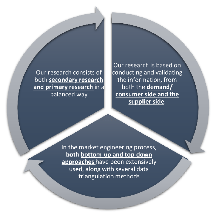
Our research design integrates both demand-side and supply-side analysis through a balanced combination of primary and secondary research methodologies. By utilizing both bottom-up and top-down approaches alongside rigorous data triangulation methods, we deliver robust market intelligence that supports strategic decision-making.
MarketGenics' comprehensive research design framework ensures the delivery of accurate, reliable, and actionable market intelligence. Through the integration of multiple research approaches, rigorous validation processes, and expert analysis, we provide our clients with the insights needed to make informed strategic decisions and capitalize on market opportunities.
MarketGenics leverages a dedicated industry panel of experts and a comprehensive suite of paid databases to effectively collect, consolidate, and analyze market intelligence.
Our approach has consistently proven to be reliable and effective in generating accurate market insights, identifying key industry trends, and uncovering emerging business opportunities.
Through both primary and secondary research, we capture and analyze critical company-level data such as manufacturing footprints, including technical centers, R&D facilities, sales offices, and headquarters.
Our expert panel further enhances our ability to estimate market size for specific brands based on validated field-level intelligence.
Our data mining techniques incorporate both parametric and non-parametric methods, allowing for structured data collection, sorting, processing, and cleaning.
Demand projections are derived from large-scale data sets analyzed through proprietary algorithms, culminating in robust and reliable market sizing.
Research Approach
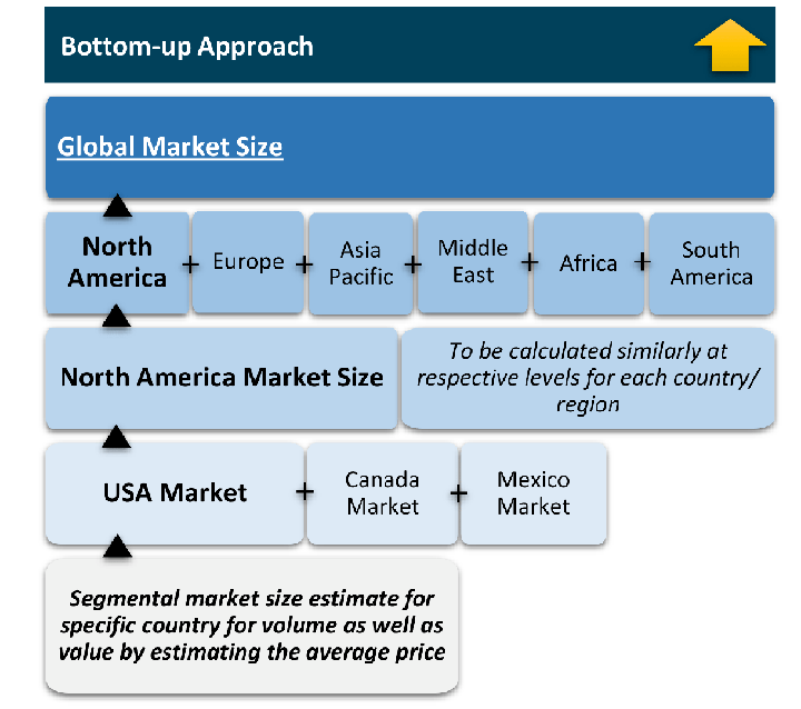
The bottom-up approach builds market estimates by starting with the smallest addressable market units and systematically aggregating them to create comprehensive market size projections.
This method begins with specific, granular data points and builds upward to create the complete market landscape.
Customer Analysis → Segmental Analysis → Geographical Analysis
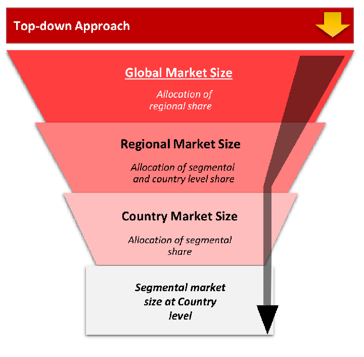
The top-down approach starts with the broadest possible market data and systematically narrows it down through a series of filters and assumptions to arrive at specific market segments or opportunities.
This method begins with the big picture and works downward to increasingly specific market slices.
TAM → SAM → SOM
Research Methods
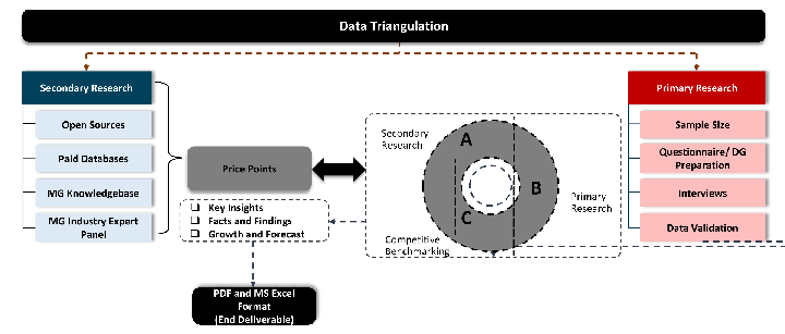
Desk / Secondary Research
While analysing the market, we extensively study secondary sources, directories, and databases to identify and collect information useful for this technical, market-oriented, and commercial report. Secondary sources that we utilize are not only the public sources, but it is a combination of Open Source, Associations, Paid Databases, MG Repository & Knowledgebase, and others.
- Company websites, annual reports, financial reports, broker reports, and investor presentations
- National government documents, statistical databases and reports
- News articles, press releases and web-casts specific to the companies operating in the market, Magazines, reports, and others
- We gather information from commercial data sources for deriving company specific data such as segmental revenue, share for geography, product revenue, and others
- Internal and external proprietary databases (industry-specific), relevant patent, and regulatory databases
- Governing Bodies, Government Organizations
- Relevant Authorities, Country-specific Associations for Industries
We also employ the model mapping approach to estimate the product level market data through the players' product portfolio
Primary Research
Primary research/ interviews is vital in analyzing the market. Most of the cases involves paid primary interviews. Primary sources include primary interviews through e-mail interactions, telephonic interviews, surveys as well as face-to-face interviews with the different stakeholders across the value chain including several industry experts.
| Type of Respondents | Number of Primaries |
|---|---|
| Tier 2/3 Suppliers | ~20 |
| Tier 1 Suppliers | ~25 |
| End-users | ~25 |
| Industry Expert/ Panel/ Consultant | ~30 |
| Total | ~100 |
MG Knowledgebase
• Repository of industry blog, newsletter and case studies
• Online platform covering detailed market reports, and company profiles
Forecasting Factors and Models
Forecasting Factors
- Historical Trends – Past market patterns, cycles, and major events that shaped how markets behave over time. Understanding past trends helps predict future behavior.
- Industry Factors – Specific characteristics of the industry like structure, regulations, and innovation cycles that affect market dynamics.
- Macroeconomic Factors – Economic conditions like GDP growth, inflation, and employment rates that affect how much money people have to spend.
- Demographic Factors – Population characteristics like age, income, and location that determine who can buy your product.
- Technology Factors – How quickly people adopt new technology and how much technology infrastructure exists.
- Regulatory Factors – Government rules, laws, and policies that can help or restrict market growth.
- Competitive Factors – Analyzing competition structure such as degree of competition and bargaining power of buyers and suppliers.
Forecasting Models / Techniques
Multiple Regression Analysis
- Identify and quantify factors that drive market changes
- Statistical modeling to establish relationships between market drivers and outcomes
Time Series Analysis – Seasonal Patterns
- Understand regular cyclical patterns in market demand
- Advanced statistical techniques to separate trend, seasonal, and irregular components
Time Series Analysis – Trend Analysis
- Identify underlying market growth patterns and momentum
- Statistical analysis of historical data to project future trends
Expert Opinion – Expert Interviews
- Gather deep industry insights and contextual understanding
- In-depth interviews with key industry stakeholders
Multi-Scenario Development
- Prepare for uncertainty by modeling different possible futures
- Creating optimistic, pessimistic, and most likely scenarios
Time Series Analysis – Moving Averages
- Sophisticated forecasting for complex time series data
- Auto-regressive integrated moving average models with seasonal components
Econometric Models
- Apply economic theory to market forecasting
- Sophisticated economic models that account for market interactions
Expert Opinion – Delphi Method
- Harness collective wisdom of industry experts
- Structured, multi-round expert consultation process
Monte Carlo Simulation
- Quantify uncertainty and probability distributions
- Thousands of simulations with varying input parameters
Research Analysis
Our research framework is built upon the fundamental principle of validating market intelligence from both demand and supply perspectives. This dual-sided approach ensures comprehensive market understanding and reduces the risk of single-source bias.
Demand-Side Analysis: We understand end-user/application behavior, preferences, and market needs along with the penetration of the product for specific application.
Supply-Side Analysis: We estimate overall market revenue, analyze the segmental share along with industry capacity, competitive landscape, and market structure.
Validation & Evaluation
Data triangulation is a validation technique that uses multiple methods, sources, or perspectives to examine the same research question, thereby increasing the credibility and reliability of research findings. In market research, triangulation serves as a quality assurance mechanism that helps identify and minimize bias, validate assumptions, and ensure accuracy in market estimates.
- Data Source Triangulation – Using multiple data sources to examine the same phenomenon
- Methodological Triangulation – Using multiple research methods to study the same research question
- Investigator Triangulation – Using multiple researchers or analysts to examine the same data
- Theoretical Triangulation – Using multiple theoretical perspectives to interpret the same data
Custom Market Research Services
We will customise the research for you, in case the report listed above does not meet your requirements.
Get 10% Free Customisation