GaN Substrate Market Size, Share & Trends Analysis Report by Wafer Size (2-inch, 4-inch, 6-inch, 8-inch and above), Substrate Type, Technology, Conductivity Type, Doping Type, Crystal Structure, Thickness, Application, Device Type, Frequency Range (for RF Applications), End-use Industry, and Geography (North America, Europe, Asia Pacific, Middle East, Africa, and South America) – Global Industry Data, Trends, and Forecasts, 2025 – 2035
|
Market Structure & Evolution |
|
|
Segmental Data Insights |
|
|
Demand Trends |
|
|
Competitive Landscape |
|
|
Strategic Development |
|
|
Future Outlook & Opportunities |
|
GaN Substrate Market Size, Share, and Growth
The global GaN substrate market is experiencing robust growth, with its estimated value of USD 0.6 billion in the year 2025 and USD 1.8 billion by the period 2035, registering a CAGR of 11.9% during the forecast period. GaN substrates are in high demand due to their high-performance and high-power, high-frequency, and high-temperature benefits that allow them to perform efficiently in powering electronics applications, RF amplifiers, and 5G infrastructure. The increasing use of electric vehicles, renewable energy solutions, and aerospace, as well as development of GaN-on-Si and GaN-on-SiC-based technologies, further boosts their adoption in the automotive, telecommunication, and defense solutions.

Mr Cheong Chee Hoo, Chairman of the NSTIC (GaN) Steering Committee said, “NSTIC (GaN) is not just a facility — it is a national platform for innovation and a catalyst for future technologies, Our goal is to build deep capabilities in GaN manufacturing and research, so that Singapore can help define the future of high-performance semiconductors.”
The growth of the global GaN substrate market is driven by increasing demand of high-efficiency power devices, development in manufacturing semiconductor and growth of electric vehicles (EVs). These demands are being met by key manufactures whose investments in research and development are enormous. As an example, Imec introduced the 300mm GaN program in October of 2025, and it is expected to increase its power device development capacity. In the same manner, Infineon declared its development toward 300mm GaN production, becoming one of the key players in the industry in terms of Integrated Device Manufacturers (IDM).
Leading companies such as Vanguard International Semiconductor and TSMC are actively advancing technological capabilities in the GaN substrate market through strategic collaborations. For instance, in January 2026, VIS entered into a technology licensing agreement with TSMC to develop both high-voltage (650V) and low-voltage (80V) GaN technologies. This partnership enables VIS to expand its GaN-on-Si platform into high-voltage applications while strengthening its overall power device portfolio. When combined with its existing GaN-on-QST platform, VIS is uniquely positioned as the only foundry globally capable of delivering GaN power technologies across both silicon and QST substrates, thereby enhancing flexibility and performance optimization for next-generation power electronics.
By the same measure, in July 2025, Infineon Technologies declared that it had successfully transferred 300 mm GaN wafer technology into its production line and that it would provide customers with samples during Q4 2025. Moreover, Sumitomo Chemical is also working on the establishment of 6-inch GaN substrates to satisfy the wafer size needs in processing power semiconductors with more than ten years of experience in mass production. The developments highlight a strategic change in the direction of big wafer sizes that are expected to enhance the manufacturing efficiency and cost reduction.
The 300mm wafers concentration indicates that the industry is willing to scale up its production in order to address the increasing demand of different fields such as power electronics and EV infrastructure. With these initiatives realising, it is likely that they will have a massive effect on the market of the GaN substrate, which will lead to innovation and improvement in the performance of power devices in the world.
The global market of the GaN substrate can be applied to adjacent markets of high-power RF amplifiers, electric vehicle power electronics, 5G and next-generation communication infrastructure, satellite and aerospace electronics, and data center power conversion systems. Diversification into other high-performance electronics will further speed up the use of GaN substrate and create an expansion in markets.
GaN Substrate Market Dynamics and Trends

Driver: Advanced Power Electronics Adoption Accelerating GaN Substrate Market Expansion
- Growth in high power electronics in automotive, telecommunications and consumer electronics markets is a core element of the growth in the market of GaN substrates. Manufacturers of electric vehicles are moving to higher power conversion efficiencies in which the GaN substrates can be used to provide better performance in terms of lower switching losses and increased thermal management.
- Modernization of telecommunications infrastructure especially 5G base stations requires radio frequency elements produced on GaN substrates because they have outstanding high-frequency performance properties. The operators of data centers are working towards achieving energy efficiency gains, and as such a move towards GaN-based power supplies is underway with much higher power densities than the traditional silicon solutions.
- In March 2024, to show their concrete industry commitment to the platform, Infineon Technologies increased their production capacity of power semiconductor with GaN technology in their Kulim facility in Malaysia, and invested heavily in the production of GaN-based power devices to charge electric vehicles and renewable energy systems.
Restraint: Substrate Manufacturing Complexity Constraining GaN Material Production Scalability
- The production of high quality GaN substrates faces high technical challenges which constrain the growth of the market and sustain high pricing systems. The crystal growth processes have very strict requirements in terms of controlled environment and long production cycles thus yielding less compared to the proven silicon wafer fabrication. The density of defects is still an issue to work on since dislocations and point defects in the crystalline structure deteriorate the performance and reliability of the device.
- The entry barriers of new manufacturers are high due to the capital-intensive nature of hydride vapor phase epitography equipment and ammonothermal growth systems. The characterization of materials requires advanced metrology equipment to guarantee that the substrate specifications are within the high device specifications.
- In August 2024, Sumitomo Electric Industries acknowledged problems with production yield in its GaN substrate factory in Itami, Japan and that further investment in process refinements and longer time to qualify its products to high-power electronic products were needed to achieve consistent production of two-inch diameter substrates with defect densities at levels below 104 cm4.
Opportunity: Emerging Quantum Computing Applications Creating Novel GaN Substrate Utilization Pathways
- The development of quantum computing technologies opens up new possibilities of GaN substrate applications in the outliers of conventional power and optoelectronics. Quantum processors based on superconducting quantum computing need cryogenic control electronics in which GaN-based devices can operate with high stability at very low temperatures. The quantum communication networks and quantum key distribution systems have shown promising qualities in single-photon sources that have been developed on the substrate of GaN.
- One application of quantum sensing uses the properties of GaN materials to design ultra-sensitive detectors that can work in the most adverse electromagnetic conditions. Technology companies and research institutions consider GaN substrates as integrated photonics platforms to provide quantum information processing platforms.
- In February 2024, Kyma Technologies stated that it would collaborate with quantum computing research laboratories to create specialized GaN substrates optimized to cryogenic electronics in operation below four Kelvins, specifically control circuitry to superconducting qubit arrays, as a strategic diversification out of the conventional power semiconductor markets.
Key Trend: Industry Consolidation Through Strategic Vertical Integration Reshaping Competitive Market Dynamics
- With several of the largest manufacturers of semiconductor devices exploring vertical integration business models, the gallium nitrate substrate business is undergoing a dramatic structural change, with large-scale manufacturers buying the specialized substrate manufacturers to ensure supply chains and in the process capture the value of the whole manufacturing ecosystem. The strategic significance of this trend of consolidation is shown by the need to control substrate production capacity as downstream uses grow and allow integrated manufacturers to streamline the epitaxial processes, decrease interdependencies, and shorten the product development cycles.
- The larger companies understand that the proprietary substrate technology offers a competitive edge in device markets that are becoming more commoditized, and that mergers and acquisitions across the entire value chain are aggressively pursued. Coherent Corp also acquired Japan-based bulk Grower of GaN substrates Sciocs Company in November 2024, and combined bulk growth of the crystal with its existing portfolio of Compound semiconductor to achieve a vertical integration of substrate manufacturing to final device manufacturing.
- This acquisition is indicative of the strategic transformation of the industry toward consolidated business models that remove weak points in the supply chain and allow closer control over the product quality, costs of production and the technological innovation paths.
GaN Substrate Market Analysis and Segmental Data

GaN-on-Silicon Carbide Substrates: The Preferred Choice for High-Performance Applications
- The GaN-on-SiC substrate segment dominates the market due to its superior material properties, well-established technology, and wide adoption in RF and power electronics. GaN-on-SiC substrates offer excellent performance, efficiency, and reliability. This can be attributed to the fact that the combination of the high breakdown voltage, wide bandgap and high thermal conductivity of GaN allow electrical breakdown to occur in the material.
- An example is Cree (Wolfspeed) and June 2025, enhanced GaN-on-SiC substrates can support next-generation electric vehicle inverters, and have an improved power density and thermal performance than conventional GaN-on-Silicon solutions. Also, GaN-on-SiC substrates are more and more demanded in 5G base station and satellite communications, where reliability in extreme conditions is very important.
- High-performance devices are driven by the prevalence of GaN-on-SiC and this is sustaining the accelerated growth in power electronics and advanced RF applications.
Asia Pacific Leading GaN Substrate Adoption Through Industrial Expansion
- Asia Pacific has the strongest demand of GaN substrates because of the accelerating growth in the electronics manufacturing industry, the growing 5G infrastructure, and the rising popularity of electric vehicles in the area. As an example, in March 2025, Sumitomo Electric Industries declared the increase in its production of the GaN-on-SiC in Japan, to provide high-end power devices to EV inverter and 5G base station companies, due to the highly developed manufacturing ecosystem and high volumes in the region.
- The presence of active government programs (such as semiconductor innovation funding programs and local manufacturing infrastructure in China, Japan, and South Korea) also enhances the market. The programs make it easy to carry out R&D, help remove bottlenecks in production, and allow quicker introduction of a GaN technologies in the consumer electronics and industrial electronics markets.
- Moreover, the domestic semiconductor projects of China have also led to the creation of wide-bandgap semiconductor capacity with China Aerospace Science and Technology Corporation (CASC) demonstrating the high-frequency RF production lines using GaN in June 2025 to serve both the commercial and defense sectors.
- The scale of manufacturing and technological investments in Asia Pacific are contributing to a very high growth resulting in the region being a key area of global GaN substrate demand.
GaN-Substrate-Market Ecosystem
The GaN substrate market is convergent on a group of vertically integrated and high-tech companies that includes Wolfspeed, Soitec (with its EpiGaN activities), IQE plc, Qorvo, Sumitomo Electric and Mitsubishi Chemical, whose size, Intellectual Property bases and manufacturing investments consolidate market power and drive technology adoption. Market leaders build on top of state-of-the-art epitaxy, larger wafer sizes, and integrated materials-to-device roadmap to win design wins in automotive and telecom and defense customers, and place barriers to entry, scaling capacity in volumes of designs.
Such players seek niche technical solutions, including Wolfspeed with its 200 mm SiC compatible processes, GaN on SiC and GaN on SiC epitaxy, IQE with its designs of tailored GaN reactor service, and Qorvo with its design of GaN MMICs, with differentiated products, such as 200 mm SiC compatible processes, base stations with its RF GaN on SiC, and an epitaxial stack optimized to be built on its GaN HEMTs. This specialization leads to performance improvement and time to market reduction of system integrators.
Integrated solutions and product diversification are the cornerstone commercial practices: companies are offering substrate supply with epitoxy, partnering with device foundries, and services to qualify customers in order to capture more value and minimize customer risk. As an example, in May 2025 IQE declared joint development programme to create 650 V GaN device stack and also increased reactor capacity to enable 8-inch GaN-on-Si development-initiatives meant to enable higher throughput and also to meet AR/VR and power OEM needs. The trends indicate that there is observable development of the larger wafer format and higher manufacturing yield, with the cost of per device becoming better and faster in adoption by sectors.

Recent Development and Strategic Overview:
- In July 2025, Incize ND Atomera, announced a strategic collaboration to enhance Gallium Nitride on Silicon (GaN-on-Si) technologies. The joint program will concentrate on optimizing GaN-on-Si device performance for high-frequency and high-power applications, with target markets in wireless infrastructure (5G/6G), satellite communications and advanced power electronics.
- In June 2025, Sumitomo Electric and Osaka Metropolitan University successfully fabricated a GaN-HEMT on a 2-inch polycrystalline diamond (PCD) substrate in a joint research project with the Japan Science and Technology Agency (JST). The GaN layer used in this study was provided by Air Water as a GaN/SiC epitaxial layer on a silicon substrate.
Report Scope
|
Attribute |
Detail |
|
Market Size in 2025 |
USD 0.6 Bn |
|
Market Forecast Value in 2035 |
USD 1.8 Bn |
|
Growth Rate (CAGR) |
11.9% |
|
Forecast Period |
2025 – 2035 |
|
Historical Data Available for |
2021 – 2024 |
|
Market Size Units |
US$ Billion for Value |
|
Report Format |
Electronic (PDF) + Excel |
|
Regions and Countries Covered |
|||||
|
North America |
Europe |
Asia Pacific |
Middle East |
Africa |
South America |
|
|
|
|
|
|
|
Companies Covered |
|||||
|
|
|
|
|
|
GaN-Substrate-Market Segmentation and Highlights
|
Segment |
Sub-segment |
|
GaN Substrate Market, By Wafer Size |
|
|
GaN Substrate Market, By Substrate Type |
|
|
GaN Substrate Market, By Technology |
|
|
GaN Substrate Market, By Conductivity Type |
|
|
GaN Substrate Market, By Doping Type |
|
|
GaN Substrate Market, By Crystal Structure |
|
|
GaN Substrate Market, By Thickness |
|
|
GaN Substrate Market, By Application |
|
|
GaN Substrate Market, By Device Type |
|
|
GaN Substrate Market, By Frequency Range (for RF Applications) |
|
|
GaN Substrate Market, By End-use Industry |
|
Frequently Asked Questions
Table of Contents
- 1. Research Methodology and Assumptions
- 1.1. Definitions
- 1.2. Research Design and Approach
- 1.3. Data Collection Methods
- 1.4. Base Estimates and Calculations
- 1.5. Forecasting Models
- 1.5.1. Key Forecast Factors & Impact Analysis
- 1.6. Secondary Research
- 1.6.1. Open Sources
- 1.6.2. Paid Databases
- 1.6.3. Associations
- 1.7. Primary Research
- 1.7.1. Primary Sources
- 1.7.2. Primary Interviews with Stakeholders across Ecosystem
- 2. Executive Summary
- 2.1. Global GaN Substrate Market Outlook
- 2.1.1. GaN Substrate Market Size (Value - US$ Bn), and Forecasts, 2021-2035
- 2.1.2. Compounded Annual Growth Rate Analysis
- 2.1.3. Growth Opportunity Analysis
- 2.1.4. Segmental Share Analysis
- 2.1.5. Geographical Share Analysis
- 2.2. Market Analysis and Facts
- 2.3. Supply-Demand Analysis
- 2.4. Competitive Benchmarking
- 2.5. Go-to- Market Strategy
- 2.5.1. Customer/ End-use Industry Assessment
- 2.5.2. Growth Opportunity Data, 2025-2035
- 2.5.2.1. Regional Data
- 2.5.2.2. Country Data
- 2.5.2.3. Segmental Data
- 2.5.3. Identification of Potential Market Spaces
- 2.5.4. GAP Analysis
- 2.5.5. Potential Attractive Price Points
- 2.5.6. Prevailing Market Risks & Challenges
- 2.5.7. Preferred Sales & Marketing Strategies
- 2.5.8. Key Recommendations and Analysis
- 2.5.9. A Way Forward
- 2.1. Global GaN Substrate Market Outlook
- 3. Industry Data and Premium Insights
- 3.1. Global GaN Substrate Industry Overview, 2025
- 3.1.1. Semiconductors & Electronics Industry Ecosystem Analysis
- 3.1.2. Key Trends for Semiconductors & Electronics Industry
- 3.1.3. Regional Distribution for Semiconductors & Electronics Industry
- 3.2. Supplier Customer Data
- 3.3. Technology Roadmap and Developments
- 3.4. Trade Analysis
- 3.4.1. Import & Export Analysis, 2025
- 3.4.2. Top Importing Countries
- 3.4.3. Top Exporting Countries
- 3.5. Trump Tariff Impact Analysis
- 3.5.1. Manufacturer
- 3.5.1.1. Based on the component & Raw material
- 3.5.2. Supply Chain
- 3.5.3. End Consumer
- 3.5.1. Manufacturer
- 3.6. Raw Material Analysis
- 3.1. Global GaN Substrate Industry Overview, 2025
- 4. Market Overview
- 4.1. Market Dynamics
- 4.1.1. Drivers
- 4.1.1.1. Rising adoption of GaN substrates in 5G infrastructure and high-frequency RF applications
- 4.1.1.2. Increasing demand from electric vehicles and renewable energy sectors for high-efficiency power devices
- 4.1.1.3. Technological advancements in GaN-on-Si and GaN-on-SiC substrates enabling superior thermal and electrical performance
- 4.1.2. Restraints
- 4.1.2.1. High manufacturing costs and complex production processes limiting widespread adoption
- 4.1.2.2. Limited availability of large-diameter wafers and challenges in scaling production for mass-market applications
- 4.1.1. Drivers
- 4.2. Key Trend Analysis
- 4.3. Regulatory Framework
- 4.3.1. Key Regulations, Norms, and Subsidies, by Key Countries
- 4.3.2. Tariffs and Standards
- 4.3.3. Impact Analysis of Regulations on the Market
- 4.4. Value Chain Analysis
- 4.5. Cost Structure Analysis
- 4.6. Pricing Analysis
- 4.7. Porter’s Five Forces Analysis
- 4.8. PESTEL Analysis
- 4.9. Global GaN Substrate Market Demand
- 4.9.1. Historical Market Size – in Value (US$ Bn), 2020-2024
- 4.9.2. Current and Future Market Size - in Value (US$ Bn), 2025–2035
- 4.9.2.1. Y-o-Y Growth Trends
- 4.9.2.2. Absolute $ Opportunity Assessment
- 4.1. Market Dynamics
- 5. Competition Landscape
- 5.1. Competition structure
- 5.1.1. Fragmented v/s consolidated
- 5.2. Company Share Analysis, 2025
- 5.2.1. Global Company Market Share
- 5.2.2. By Region
- 5.2.2.1. North America
- 5.2.2.2. Europe
- 5.2.2.3. Asia Pacific
- 5.2.2.4. Middle East
- 5.2.2.5. Africa
- 5.2.2.6. South America
- 5.3. Product Comparison Matrix
- 5.3.1. Specifications
- 5.3.2. Market Positioning
- 5.3.3. Pricing
- 5.1. Competition structure
- 6. Global GaN Substrate Market Analysis, by Wafer Size
- 6.1. Key Segment Analysis
- 6.2. GaN Substrate Market Size (Value - US$ Bn), Analysis, and Forecasts, by Wafer Size, 2021-2035
- 6.2.1. 2-inch
- 6.2.2. 4-inch
- 6.2.3. 6-inch
- 6.2.4. 8-inch and above
- 7. Global GaN Substrate Market Analysis, by Substrate Type
- 7.1. Key Segment Analysis
- 7.2. GaN Substrate Market Size (Value - US$ Bn), Analysis, and Forecasts, by Substrate Type, 2021-2035
- 7.2.1. GaN-on-Sapphire
- 7.2.2. GaN-on-Silicon (GaN-on-Si)
- 7.2.3. GaN-on-Silicon Carbide (GaN-on-SiC)
- 7.2.4. GaN-on-GaN (Freestanding GaN)
- 7.2.5. GaN-on-Diamond
- 7.2.6. Others
- 8. Global GaN Substrate Market Analysis, by Technology
- 8.1. Key Segment Analysis
- 8.2. GaN Substrate Market Size (Value - US$ Bn), Analysis, and Forecasts, by Technology, 2021-2035
- 8.2.1. Hydride Vapor Phase Epitaxy (HVPE)
- 8.2.2. Metal-Organic Chemical Vapor Deposition (MOCVD)
- 8.2.3. Molecular Beam Epitaxy (MBE)
- 8.2.4. Ammonothermal Method
- 8.2.5. Others
- 9. Global GaN Substrate Market Analysis, by Conductivity Type
- 9.1. Key Segment Analysis
- 9.2. GaN Substrate Market Size (Value - US$ Bn), Analysis, and Forecasts, by Conductivity Type, 2021-2035
- 9.2.1. N-type
- 9.2.2. P-type
- 9.2.3. Semi-insulating
- 10. Global GaN Substrate Market Analysis, by Doping Type
- 10.1. Key Segment Analysis
- 10.2. GaN Substrate Market Size (Value - US$ Bn), Analysis, and Forecasts, by Doping Type, 2021-2035
- 10.2.1. Doped
- 10.2.2. Undoped
- 11. Global GaN Substrate Market Analysis, by Crystal Structure
- 11.1. Key Segment Analysis
- 11.2. GaN Substrate Market Size (Value - US$ Bn), Analysis, and Forecasts, by Crystal Structure, 2021-2035
- 11.2.1. Wurtzite Structure
- 11.2.2. Zinc Blende Structure
- 12. Global GaN Substrate Market Analysis, by Thickness
- 12.1. Key Segment Analysis
- 12.2. GaN Substrate Market Size (Value - US$ Bn), Analysis, and Forecasts, by Thickness, 2021-2035
- 12.2.1. Less than 300 μm
- 12.2.2. 300-500 μm
- 12.2.3. 500-1000 μm
- 12.2.4. Above 1000 μm
- 13. Global GaN Substrate Market Analysis, by Application
- 13.1. Key Segment Analysis
- 13.2. GaN Substrate Market Size (Value - US$ Bn), Analysis, and Forecasts, by Application, 2021-2035
- 13.2.1. Power Electronics
- 13.2.2. Radio Frequency (RF) Devices
- 13.2.3. Optoelectronics
- 13.2.4. Others
- 14. Global GaN Substrate Market Analysis, by Device Type
- 14.1. Key Findings
- 14.2. GaN Substrate Market Size (Volume - Units and Value - US$ Mn), Analysis, and Forecasts, by Device Type, 2021-2035
- 14.2.1. High Electron Mobility Transistors (HEMTs)
- 14.2.2. Light Emitting Diodes (LEDs)
- 14.2.3. Laser Diodes (LDs)
- 14.2.4. RF Amplifiers
- 14.2.5. Power Modules
- 14.2.6. Rectifiers
- 14.2.7. Others
- 15. Global GaN Substrate Market Analysis, by Frequency Range (for RF Applications)
- 15.1. Key Findings
- 15.2. GaN Substrate Market Size (Volume - Units and Value - US$ Mn), Analysis, and Forecasts, by Frequency Range (for RF Applications), 2021-2035
- 15.2.1. Below 6 GHz
- 15.2.2. 6-30 GHz
- 15.2.3. Above 30 GHz
- 16. Global GaN Substrate Market Analysis, by End-use Industry
- 16.1. Key Findings
- 16.2. GaN Substrate Market Size (Volume - Units and Value - US$ Mn), Analysis, and Forecasts, by End-use Industry, 2021-2035
- 16.2.1. Consumer Electronics
- 16.2.1.1. Smartphones
- 16.2.1.2. Laptops & Tablets
- 16.2.1.3. Fast Chargers & Adapters
- 16.2.1.4. Wireless Charging Systems
- 16.2.1.5. Gaming Consoles
- 16.2.1.6. Wearable Devices
- 16.2.1.7. Display Backlighting
- 16.2.1.8. Others
- 16.2.2. Automotive
- 16.2.2.1. Electric Vehicle (EV) Powertrains
- 16.2.2.2. On-Board Chargers (OBC)
- 16.2.2.3. DC-DC Converters
- 16.2.2.4. Battery Management Systems
- 16.2.2.5. LiDAR Systems
- 16.2.2.6. Automotive Lighting (LED Headlights)
- 16.2.2.7. Vehicle-to-Everything (V2X) Communication
- 16.2.2.8. Others
- 16.2.3. Telecommunications
- 16.2.3.1. 5G Base Stations
- 16.2.3.2. Small Cell Infrastructure
- 16.2.3.3. Massive MIMO Systems
- 16.2.3.4. Satellite Communication
- 16.2.3.5. Fiber Optic Communication
- 16.2.3.6. Network Equipment
- 16.2.3.7. RF Front-End Modules
- 16.2.3.8. Others
- 16.2.4. Aerospace & Defense
- 16.2.4.1. Radar Systems
- 16.2.4.2. Electronic Warfare Systems
- 16.2.4.3. Satellite Communication Systems
- 16.2.4.4. Avionics
- 16.2.4.5. Missile Guidance Systems
- 16.2.4.6. Military Communication Equipment
- 16.2.4.7. Space Applications
- 16.2.4.8. Others
- 16.2.5. Industrial
- 16.2.5.1. Motor Drives
- 16.2.5.2. Industrial Power Supplies
- 16.2.5.3. Solar Inverters
- 16.2.5.4. UPS Systems
- 16.2.5.5. Welding Equipment
- 16.2.5.6. Industrial Lighting
- 16.2.5.7. Robotics & Automation
- 16.2.5.8. Others
- 16.2.6. Energy & Power
- 16.2.6.1. Grid Infrastructure
- 16.2.6.2. Smart Grid Systems
- 16.2.6.3. Energy Storage Systems
- 16.2.6.4. Wind Turbine Converters
- 16.2.6.5. Solar Power Systems
- 16.2.6.6. Electric Power Distribution
- 16.2.6.7. High Voltage Direct Current (HVDC) Systems
- 16.2.6.8. Others
- 16.2.7. Medical & Healthcare
- 16.2.7.1. Medical Imaging Equipment
- 16.2.7.2. Surgical Instruments
- 16.2.7.3. Patient Monitoring Systems
- 16.2.7.4. UV Sterilization Systems
- 16.2.7.5. Diagnostic Equipment
- 16.2.7.6. Therapeutic Devices
- 16.2.7.7. Others
- 16.2.8. Data Centers & IT Infrastructure
- 16.2.8.1. Server Power Supplies
- 16.2.8.2. Data Center UPS
- 16.2.8.3. High-Efficiency Power Conversion
- 16.2.8.4. Cooling Systems
- 16.2.8.5. Network Switches & Routers
- 16.2.8.6. Others
- 16.2.9. Computing & Gaming
- 16.2.9.1. High-Performance Computing
- 16.2.9.2. Graphics Processing Units (GPUs)
- 16.2.9.3. Gaming Hardware
- 16.2.9.4. Data Processing Equipment
- 16.2.9.5. Quantum Computing Infrastructure
- 16.2.9.6. Others
- 16.2.10. Other End-users
- 16.2.1. Consumer Electronics
- 17. Global GaN Substrate Market Analysis, by Region
- 17.1. Key Findings
- 17.2. GaN Substrate Market Size (Volume - Units and Value - US$ Mn), Analysis, and Forecasts, by Region, 2021-2035
- 17.2.1. North America
- 17.2.2. Europe
- 17.2.3. Asia Pacific
- 17.2.4. Middle East
- 17.2.5. Africa
- 17.2.6. South America
- 18. North America GaN Substrate Market Analysis
- 18.1. Key Segment Analysis
- 18.2. Regional Snapshot
- 18.3. North America GaN Substrate Market Size Value - US$ Bn), Analysis, and Forecasts, 2021-2035
- 18.3.1. Wafer Size
- 18.3.2. Substrate Type
- 18.3.3. Technology
- 18.3.4. Conductivity Type
- 18.3.5. Doping Type
- 18.3.6. Crystal Structure
- 18.3.7. Thickness
- 18.3.8. Application
- 18.3.9. Device Type
- 18.3.10. Frequency Range (for RF Applications)
- 18.3.11. End-use Industry
- 18.3.12. Country
- 18.3.12.1. USA
- 18.3.12.2. Canada
- 18.3.12.3. Mexico
- 18.4. USA GaN Substrate Market
- 18.4.1. Country Segmental Analysis
- 18.4.2. Wafer Size
- 18.4.3. Substrate Type
- 18.4.4. Technology
- 18.4.5. Conductivity Type
- 18.4.6. Doping Type
- 18.4.7. Crystal Structure
- 18.4.8. Thickness
- 18.4.9. Application
- 18.4.10. Device Type
- 18.4.11. Frequency Range (for RF Applications)
- 18.4.12. End-use Industry
- 18.5. Canada GaN Substrate Market
- 18.5.1. Country Segmental Analysis
- 18.5.2. Wafer Size
- 18.5.3. Substrate Type
- 18.5.4. Technology
- 18.5.5. Conductivity Type
- 18.5.6. Doping Type
- 18.5.7. Crystal Structure
- 18.5.8. Thickness
- 18.5.9. Application
- 18.5.10. Device Type
- 18.5.11. Frequency Range (for RF Applications)
- 18.5.12. End-use Industry
- 18.6. Mexico GaN Substrate Market
- 18.6.1. Country Segmental Analysis
- 18.6.2. Wafer Size
- 18.6.3. Substrate Type
- 18.6.4. Technology
- 18.6.5. Conductivity Type
- 18.6.6. Doping Type
- 18.6.7. Crystal Structure
- 18.6.8. Thickness
- 18.6.9. Application
- 18.6.10. Device Type
- 18.6.11. Frequency Range (for RF Applications)
- 18.6.12. End-use Industry
- 19. Europe GaN Substrate Market Analysis
- 19.1. Key Segment Analysis
- 19.2. Regional Snapshot
- 19.3. Europe GaN Substrate Market Size (Value - US$ Bn), Analysis, and Forecasts, 2021-2035
- 19.3.1. Wafer Size
- 19.3.2. Substrate Type
- 19.3.3. Technology
- 19.3.4. Conductivity Type
- 19.3.5. Doping Type
- 19.3.6. Crystal Structure
- 19.3.7. Thickness
- 19.3.8. Application
- 19.3.9. Device Type
- 19.3.10. Frequency Range (for RF Applications)
- 19.3.11. End-use Industry
- 19.3.12. Country
- 19.3.12.1. Germany
- 19.3.12.2. United Kingdom
- 19.3.12.3. France
- 19.3.12.4. Italy
- 19.3.12.5. Spain
- 19.3.12.6. Netherlands
- 19.3.12.7. Nordic Countries
- 19.3.12.8. Poland
- 19.3.12.9. Russia & CIS
- 19.3.12.10. Rest of Europe
- 19.4. Germany GaN Substrate Market
- 19.4.1. Country Segmental Analysis
- 19.4.2. Wafer Size
- 19.4.3. Substrate Type
- 19.4.4. Technology
- 19.4.5. Conductivity Type
- 19.4.6. Doping Type
- 19.4.7. Crystal Structure
- 19.4.8. Thickness
- 19.4.9. Application
- 19.4.10. Device Type
- 19.4.11. Frequency Range (for RF Applications)
- 19.4.12. End-use Industry
- 19.5. United Kingdom GaN Substrate Market
- 19.5.1. Country Segmental Analysis
- 19.5.2. Wafer Size
- 19.5.3. Substrate Type
- 19.5.4. Technology
- 19.5.5. Conductivity Type
- 19.5.6. Doping Type
- 19.5.7. Crystal Structure
- 19.5.8. Thickness
- 19.5.9. Application
- 19.5.10. Device Type
- 19.5.11. Frequency Range (for RF Applications)
- 19.5.12. End-use Industry
- 19.6. France GaN Substrate Market
- 19.6.1. Country Segmental Analysis
- 19.6.2. Wafer Size
- 19.6.3. Substrate Type
- 19.6.4. Technology
- 19.6.5. Conductivity Type
- 19.6.6. Doping Type
- 19.6.7. Crystal Structure
- 19.6.8. Thickness
- 19.6.9. Application
- 19.6.10. Device Type
- 19.6.11. Frequency Range (for RF Applications)
- 19.6.12. End-use Industry
- 19.7. Italy GaN Substrate Market
- 19.7.1. Country Segmental Analysis
- 19.7.2. Wafer Size
- 19.7.3. Substrate Type
- 19.7.4. Technology
- 19.7.5. Conductivity Type
- 19.7.6. Doping Type
- 19.7.7. Crystal Structure
- 19.7.8. Thickness
- 19.7.9. Application
- 19.7.10. Device Type
- 19.7.11. Frequency Range (for RF Applications)
- 19.7.12. End-use Industry
- 19.8. Spain GaN Substrate Market
- 19.8.1. Country Segmental Analysis
- 19.8.2. Wafer Size
- 19.8.3. Substrate Type
- 19.8.4. Technology
- 19.8.5. Conductivity Type
- 19.8.6. Doping Type
- 19.8.7. Crystal Structure
- 19.8.8. Thickness
- 19.8.9. Application
- 19.8.10. Device Type
- 19.8.11. Frequency Range (for RF Applications)
- 19.8.12. End-use Industry
- 19.9. Netherlands GaN Substrate Market
- 19.9.1. Country Segmental Analysis
- 19.9.2. Wafer Size
- 19.9.3. Substrate Type
- 19.9.4. Technology
- 19.9.5. Conductivity Type
- 19.9.6. Doping Type
- 19.9.7. Crystal Structure
- 19.9.8. Thickness
- 19.9.9. Application
- 19.9.10. Device Type
- 19.9.11. Frequency Range (for RF Applications)
- 19.9.12. End-use Industry
- 19.10. Nordic Countries GaN Substrate Market
- 19.10.1. Country Segmental Analysis
- 19.10.2. Wafer Size
- 19.10.3. Substrate Type
- 19.10.4. Technology
- 19.10.5. Conductivity Type
- 19.10.6. Doping Type
- 19.10.7. Crystal Structure
- 19.10.8. Thickness
- 19.10.9. Application
- 19.10.10. Device Type
- 19.10.11. Frequency Range (for RF Applications)
- 19.10.12. End-use Industry
- 19.11. Poland GaN Substrate Market
- 19.11.1. Country Segmental Analysis
- 19.11.2. Wafer Size
- 19.11.3. Substrate Type
- 19.11.4. Technology
- 19.11.5. Conductivity Type
- 19.11.6. Doping Type
- 19.11.7. Crystal Structure
- 19.11.8. Thickness
- 19.11.9. Application
- 19.11.10. Device Type
- 19.11.11. Frequency Range (for RF Applications)
- 19.11.12. End-use Industry
- 19.12. Russia & CIS GaN Substrate Market
- 19.12.1. Country Segmental Analysis
- 19.12.2. Wafer Size
- 19.12.3. Substrate Type
- 19.12.4. Technology
- 19.12.5. Conductivity Type
- 19.12.6. Doping Type
- 19.12.7. Crystal Structure
- 19.12.8. Thickness
- 19.12.9. Application
- 19.12.10. Device Type
- 19.12.11. Frequency Range (for RF Applications)
- 19.12.12. End-use Industry
- 19.13. Rest of Europe GaN Substrate Market
- 19.13.1. Country Segmental Analysis
- 19.13.2. Wafer Size
- 19.13.3. Substrate Type
- 19.13.4. Technology
- 19.13.5. Conductivity Type
- 19.13.6. Doping Type
- 19.13.7. Crystal Structure
- 19.13.8. Thickness
- 19.13.9. Application
- 19.13.10. Device Type
- 19.13.11. Frequency Range (for RF Applications)
- 19.13.12. End-use Industry
- 20. Asia Pacific GaN Substrate Market Analysis
- 20.1. Key Segment Analysis
- 20.2. Regional Snapshot
- 20.3. East Asia GaN Substrate Market Size (Value - US$ Bn), Analysis, and Forecasts, 2021-2035
- 20.3.1. Wafer Size
- 20.3.2. Substrate Type
- 20.3.3. Technology
- 20.3.4. Conductivity Type
- 20.3.5. Doping Type
- 20.3.6. Crystal Structure
- 20.3.7. Thickness
- 20.3.8. Application
- 20.3.9. Device Type
- 20.3.10. Frequency Range (for RF Applications)
- 20.3.11. End-use Industry
- 20.3.12. Country
- 20.3.12.1. China
- 20.3.12.2. India
- 20.3.12.3. Japan
- 20.3.12.4. South Korea
- 20.3.12.5. Australia and New Zealand
- 20.3.12.6. Indonesia
- 20.3.12.7. Malaysia
- 20.3.12.8. Thailand
- 20.3.12.9. Vietnam
- 20.3.12.10. Rest of Asia Pacific
- 20.4. China GaN Substrate Market
- 20.4.1. Country Segmental Analysis
- 20.4.2. Wafer Size
- 20.4.3. Substrate Type
- 20.4.4. Technology
- 20.4.5. Conductivity Type
- 20.4.6. Doping Type
- 20.4.7. Crystal Structure
- 20.4.8. Thickness
- 20.4.9. Application
- 20.4.10. Device Type
- 20.4.11. Frequency Range (for RF Applications)
- 20.4.12. End-use Industry
- 20.5. India GaN Substrate Market
- 20.5.1. Country Segmental Analysis
- 20.5.2. Wafer Size
- 20.5.3. Substrate Type
- 20.5.4. Technology
- 20.5.5. Conductivity Type
- 20.5.6. Doping Type
- 20.5.7. Crystal Structure
- 20.5.8. Thickness
- 20.5.9. Application
- 20.5.10. Device Type
- 20.5.11. Frequency Range (for RF Applications)
- 20.5.12. End-use Industry
- 20.6. Japan GaN Substrate Market
- 20.6.1. Country Segmental Analysis
- 20.6.2. Wafer Size
- 20.6.3. Substrate Type
- 20.6.4. Technology
- 20.6.5. Conductivity Type
- 20.6.6. Doping Type
- 20.6.7. Crystal Structure
- 20.6.8. Thickness
- 20.6.9. Application
- 20.6.10. Device Type
- 20.6.11. Frequency Range (for RF Applications)
- 20.6.12. End-use Industry
- 20.7. South Korea GaN Substrate Market
- 20.7.1. Country Segmental Analysis
- 20.7.2. Wafer Size
- 20.7.3. Substrate Type
- 20.7.4. Technology
- 20.7.5. Conductivity Type
- 20.7.6. Doping Type
- 20.7.7. Crystal Structure
- 20.7.8. Thickness
- 20.7.9. Application
- 20.7.10. Device Type
- 20.7.11. Frequency Range (for RF Applications)
- 20.7.12. End-use Industry
- 20.8. Australia and New Zealand GaN Substrate Market
- 20.8.1. Country Segmental Analysis
- 20.8.2. Wafer Size
- 20.8.3. Substrate Type
- 20.8.4. Technology
- 20.8.5. Conductivity Type
- 20.8.6. Doping Type
- 20.8.7. Crystal Structure
- 20.8.8. Thickness
- 20.8.9. Application
- 20.8.10. Device Type
- 20.8.11. Frequency Range (for RF Applications)
- 20.8.12. End-use Industry
- 20.9. Indonesia GaN Substrate Market
- 20.9.1. Country Segmental Analysis
- 20.9.2. Wafer Size
- 20.9.3. Substrate Type
- 20.9.4. Technology
- 20.9.5. Conductivity Type
- 20.9.6. Doping Type
- 20.9.7. Crystal Structure
- 20.9.8. Thickness
- 20.9.9. Application
- 20.9.10. Device Type
- 20.9.11. Frequency Range (for RF Applications)
- 20.9.12. End-use Industry
- 20.10. Malaysia GaN Substrate Market
- 20.10.1. Country Segmental Analysis
- 20.10.2. Wafer Size
- 20.10.3. Substrate Type
- 20.10.4. Technology
- 20.10.5. Conductivity Type
- 20.10.6. Doping Type
- 20.10.7. Crystal Structure
- 20.10.8. Thickness
- 20.10.9. Application
- 20.10.10. Device Type
- 20.10.11. Frequency Range (for RF Applications)
- 20.10.12. End-use Industry
- 20.11. Thailand GaN Substrate Market
- 20.11.1. Country Segmental Analysis
- 20.11.2. Wafer Size
- 20.11.3. Substrate Type
- 20.11.4. Technology
- 20.11.5. Conductivity Type
- 20.11.6. Doping Type
- 20.11.7. Crystal Structure
- 20.11.8. Thickness
- 20.11.9. Application
- 20.11.10. Device Type
- 20.11.11. Frequency Range (for RF Applications)
- 20.11.12. End-use Industry
- 20.12. Vietnam GaN Substrate Market
- 20.12.1. Country Segmental Analysis
- 20.12.2. Wafer Size
- 20.12.3. Substrate Type
- 20.12.4. Technology
- 20.12.5. Conductivity Type
- 20.12.6. Doping Type
- 20.12.7. Crystal Structure
- 20.12.8. Thickness
- 20.12.9. Application
- 20.12.10. Device Type
- 20.12.11. Frequency Range (for RF Applications)
- 20.12.12. End-use Industry
- 20.13. Rest of Asia Pacific GaN Substrate Market
- 20.13.1. Country Segmental Analysis
- 20.13.2. Wafer Size
- 20.13.3. Substrate Type
- 20.13.4. Technology
- 20.13.5. Conductivity Type
- 20.13.6. Doping Type
- 20.13.7. Crystal Structure
- 20.13.8. Thickness
- 20.13.9. Application
- 20.13.10. Device Type
- 20.13.11. Frequency Range (for RF Applications)
- 20.13.12. End-use Industry
- 21. Middle East GaN Substrate Market Analysis
- 21.1. Key Segment Analysis
- 21.2. Regional Snapshot
- 21.3. Middle East GaN Substrate Market Size (Value - US$ Bn), Analysis, and Forecasts, 2021-2035
- 21.3.1. Wafer Size
- 21.3.2. Substrate Type
- 21.3.3. Technology
- 21.3.4. Conductivity Type
- 21.3.5. Doping Type
- 21.3.6. Crystal Structure
- 21.3.7. Thickness
- 21.3.8. Application
- 21.3.9. Device Type
- 21.3.10. Frequency Range (for RF Applications)
- 21.3.11. End-use Industry
- 21.3.12. Country
- 21.3.12.1. Turkey
- 21.3.12.2. UAE
- 21.3.12.3. Saudi Arabia
- 21.3.12.4. Israel
- 21.3.12.5. Rest of Middle East
- 21.4. Turkey GaN Substrate Market
- 21.4.1. Country Segmental Analysis
- 21.4.2. Wafer Size
- 21.4.3. Substrate Type
- 21.4.4. Technology
- 21.4.5. Conductivity Type
- 21.4.6. Doping Type
- 21.4.7. Crystal Structure
- 21.4.8. Thickness
- 21.4.9. Application
- 21.4.10. Device Type
- 21.4.11. Frequency Range (for RF Applications)
- 21.4.12. End-use Industry
- 21.5. UAE GaN Substrate Market
- 21.5.1. Country Segmental Analysis
- 21.5.2. Wafer Size
- 21.5.3. Substrate Type
- 21.5.4. Technology
- 21.5.5. Conductivity Type
- 21.5.6. Doping Type
- 21.5.7. Crystal Structure
- 21.5.8. Thickness
- 21.5.9. Application
- 21.5.10. Device Type
- 21.5.11. Frequency Range (for RF Applications)
- 21.5.12. End-use Industry
- 21.6. Saudi Arabia GaN Substrate Market
- 21.6.1. Country Segmental Analysis
- 21.6.2. Wafer Size
- 21.6.3. Substrate Type
- 21.6.4. Technology
- 21.6.5. Conductivity Type
- 21.6.6. Doping Type
- 21.6.7. Crystal Structure
- 21.6.8. Thickness
- 21.6.9. Application
- 21.6.10. Device Type
- 21.6.11. Frequency Range (for RF Applications)
- 21.6.12. End-use Industry
- 21.7. Israel GaN Substrate Market
- 21.7.1. Country Segmental Analysis
- 21.7.2. Wafer Size
- 21.7.3. Substrate Type
- 21.7.4. Technology
- 21.7.5. Conductivity Type
- 21.7.6. Doping Type
- 21.7.7. Crystal Structure
- 21.7.8. Thickness
- 21.7.9. Application
- 21.7.10. Device Type
- 21.7.11. Frequency Range (for RF Applications)
- 21.7.12. End-use Industry
- 21.8. Rest of Middle East GaN Substrate Market
- 21.8.1. Country Segmental Analysis
- 21.8.2. Wafer Size
- 21.8.3. Substrate Type
- 21.8.4. Technology
- 21.8.5. Conductivity Type
- 21.8.6. Doping Type
- 21.8.7. Crystal Structure
- 21.8.8. Thickness
- 21.8.9. Application
- 21.8.10. Device Type
- 21.8.11. Frequency Range (for RF Applications)
- 21.8.12. End-use Industry
- 22. Africa GaN Substrate Market Analysis
- 22.1. Key Segment Analysis
- 22.2. Regional Snapshot
- 22.3. Africa GaN Substrate Market Size (Value - US$ Bn), Analysis, and Forecasts, 2021-2035
- 22.3.1. Wafer Size
- 22.3.2. Substrate Type
- 22.3.3. Technology
- 22.3.4. Conductivity Type
- 22.3.5. Doping Type
- 22.3.6. Crystal Structure
- 22.3.7. Thickness
- 22.3.8. Application
- 22.3.9. Device Type
- 22.3.10. Frequency Range (for RF Applications)
- 22.3.11. End-use Industry
- 22.3.12. Country
- 22.3.12.1. South Africa
- 22.3.12.2. Egypt
- 22.3.12.3. Nigeria
- 22.3.12.4. Algeria
- 22.3.12.5. Rest of Africa
- 22.4. South Africa GaN Substrate Market
- 22.4.1. Country Segmental Analysis
- 22.4.2. Wafer Size
- 22.4.3. Substrate Type
- 22.4.4. Technology
- 22.4.5. Conductivity Type
- 22.4.6. Doping Type
- 22.4.7. Crystal Structure
- 22.4.8. Thickness
- 22.4.9. Application
- 22.4.10. Device Type
- 22.4.11. Frequency Range (for RF Applications)
- 22.4.12. End-use Industry
- 22.5. Egypt GaN Substrate Market
- 22.5.1. Country Segmental Analysis
- 22.5.2. Wafer Size
- 22.5.3. Substrate Type
- 22.5.4. Technology
- 22.5.5. Conductivity Type
- 22.5.6. Doping Type
- 22.5.7. Crystal Structure
- 22.5.8. Thickness
- 22.5.9. Application
- 22.5.10. Device Type
- 22.5.11. Frequency Range (for RF Applications)
- 22.5.12. End-use Industry
- 22.6. Nigeria GaN Substrate Market
- 22.6.1. Country Segmental Analysis
- 22.6.2. Wafer Size
- 22.6.3. Substrate Type
- 22.6.4. Technology
- 22.6.5. Conductivity Type
- 22.6.6. Doping Type
- 22.6.7. Crystal Structure
- 22.6.8. Thickness
- 22.6.9. Application
- 22.6.10. Device Type
- 22.6.11. Frequency Range (for RF Applications)
- 22.6.12. End-use Industry
- 22.7. Algeria GaN Substrate Market
- 22.7.1. Country Segmental Analysis
- 22.7.2. Wafer Size
- 22.7.3. Substrate Type
- 22.7.4. Technology
- 22.7.5. Conductivity Type
- 22.7.6. Doping Type
- 22.7.7. Crystal Structure
- 22.7.8. Thickness
- 22.7.9. Application
- 22.7.10. Device Type
- 22.7.11. Frequency Range (for RF Applications)
- 22.7.12. End-use Industry
- 22.8. Rest of Africa GaN Substrate Market
- 22.8.1. Country Segmental Analysis
- 22.8.2. Wafer Size
- 22.8.3. Substrate Type
- 22.8.4. Technology
- 22.8.5. Conductivity Type
- 22.8.6. Doping Type
- 22.8.7. Crystal Structure
- 22.8.8. Thickness
- 22.8.9. Application
- 22.8.10. Device Type
- 22.8.11. Frequency Range (for RF Applications)
- 22.8.12. End-use Industry
- 23. South America GaN Substrate Market Analysis
- 23.1. Key Segment Analysis
- 23.2. Regional Snapshot
- 23.3. Central and South Africa GaN Substrate Market Size (Value - US$ Bn), Analysis, and Forecasts, 2021-2035
- 23.3.1. Wafer Size
- 23.3.2. Substrate Type
- 23.3.3. Technology
- 23.3.4. Conductivity Type
- 23.3.5. Doping Type
- 23.3.6. Crystal Structure
- 23.3.7. Thickness
- 23.3.8. Application
- 23.3.9. Device Type
- 23.3.10. Frequency Range (for RF Applications)
- 23.3.11. End-use Industry
- 23.3.12. Country
- 23.3.12.1. Brazil
- 23.3.12.2. Argentina
- 23.3.12.3. Rest of South America
- 23.4. Brazil GaN Substrate Market
- 23.4.1. Country Segmental Analysis
- 23.4.2. Wafer Size
- 23.4.3. Substrate Type
- 23.4.4. Technology
- 23.4.5. Conductivity Type
- 23.4.6. Doping Type
- 23.4.7. Crystal Structure
- 23.4.8. Thickness
- 23.4.9. Application
- 23.4.10. Device Type
- 23.4.11. Frequency Range (for RF Applications)
- 23.4.12. End-use Industry
- 23.5. Argentina GaN Substrate Market
- 23.5.1. Country Segmental Analysis
- 23.5.2. Wafer Size
- 23.5.3. Substrate Type
- 23.5.4. Technology
- 23.5.5. Conductivity Type
- 23.5.6. Doping Type
- 23.5.7. Crystal Structure
- 23.5.8. Thickness
- 23.5.9. Application
- 23.5.10. Device Type
- 23.5.11. Frequency Range (for RF Applications)
- 23.5.12. End-use Industry
- 23.6. Rest of South America GaN Substrate Market
- 23.6.1. Country Segmental Analysis
- 23.6.2. Wafer Size
- 23.6.3. Substrate Type
- 23.6.4. Technology
- 23.6.5. Conductivity Type
- 23.6.6. Doping Type
- 23.6.7. Crystal Structure
- 23.6.8. Thickness
- 23.6.9. Application
- 23.6.10. Device Type
- 23.6.11. Frequency Range (for RF Applications)
- 23.6.12. End-use Industry
- 24. Key Players/ Company Profile
- 24.1. DOWA Electronics Materials
- 24.1.1. Company Details/ Overview
- 24.1.2. Company Financials
- 24.1.3. Key Customers and Competitors
- 24.1.4. Business/ Industry Portfolio
- 24.1.5. Product Portfolio/ Specification Details
- 24.1.6. Pricing Data
- 24.1.7. Strategic Overview
- 24.1.8. Recent Developments
- 24.2. Enkris Semiconductor
- 24.3. EpiGaN (Soitec subsidiary)
- 24.4. Eta Research
- 24.5. GLC Semiconductor Group
- 24.6. IQE plc
- 24.7. Kyma Technologies
- 24.8. LumiGNtech co., Ltd.
- 24.9. Mitsubishi Chemical Corporation
- 24.10. MSE Supplies LLC
- 24.11. Nanowin Technology
- 24.12. Nitride Semiconductors Co., Ltd.
- 24.13. PAM-XIAMEN
- 24.14. Qorvo
- 24.15. Saint-Gobain
- 24.16. Sciocs Company Limited
- 24.17. Semiconductor Wafer Inc.
- 24.18. Sino Nitride Semiconductor
- 24.19. Soitec
- 24.20. Sumitomo Electric Industries, Ltd.
- 24.21. Suzhou Nanowin Science and Technology
- 24.22. Wolfspeed, Inc.
- 24.23. Xiamen Powerway Advanced Material Co., Ltd.
- 24.24. Other Key Players
- 24.1. DOWA Electronics Materials
Note* - This is just tentative list of players. While providing the report, we will cover more number of players based on their revenue and share for each geography
Research Design
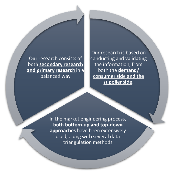
Our research design integrates both demand-side and supply-side analysis through a balanced combination of primary and secondary research methodologies. By utilizing both bottom-up and top-down approaches alongside rigorous data triangulation methods, we deliver robust market intelligence that supports strategic decision-making.
MarketGenics' comprehensive research design framework ensures the delivery of accurate, reliable, and actionable market intelligence. Through the integration of multiple research approaches, rigorous validation processes, and expert analysis, we provide our clients with the insights needed to make informed strategic decisions and capitalize on market opportunities.
MarketGenics leverages a dedicated industry panel of experts and a comprehensive suite of paid databases to effectively collect, consolidate, and analyze market intelligence.
Our approach has consistently proven to be reliable and effective in generating accurate market insights, identifying key industry trends, and uncovering emerging business opportunities.
Through both primary and secondary research, we capture and analyze critical company-level data such as manufacturing footprints, including technical centers, R&D facilities, sales offices, and headquarters.
Our expert panel further enhances our ability to estimate market size for specific brands based on validated field-level intelligence.
Our data mining techniques incorporate both parametric and non-parametric methods, allowing for structured data collection, sorting, processing, and cleaning.
Demand projections are derived from large-scale data sets analyzed through proprietary algorithms, culminating in robust and reliable market sizing.
Research Approach
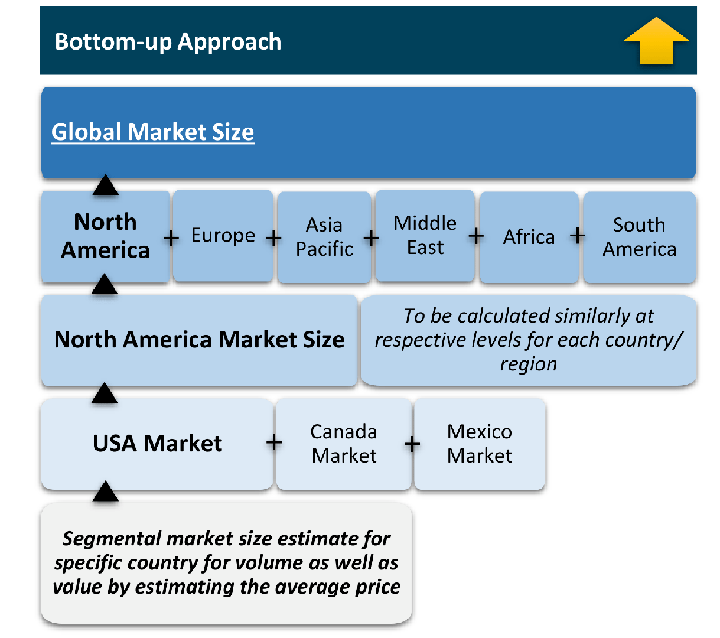
The bottom-up approach builds market estimates by starting with the smallest addressable market units and systematically aggregating them to create comprehensive market size projections.
This method begins with specific, granular data points and builds upward to create the complete market landscape.
Customer Analysis → Segmental Analysis → Geographical Analysis
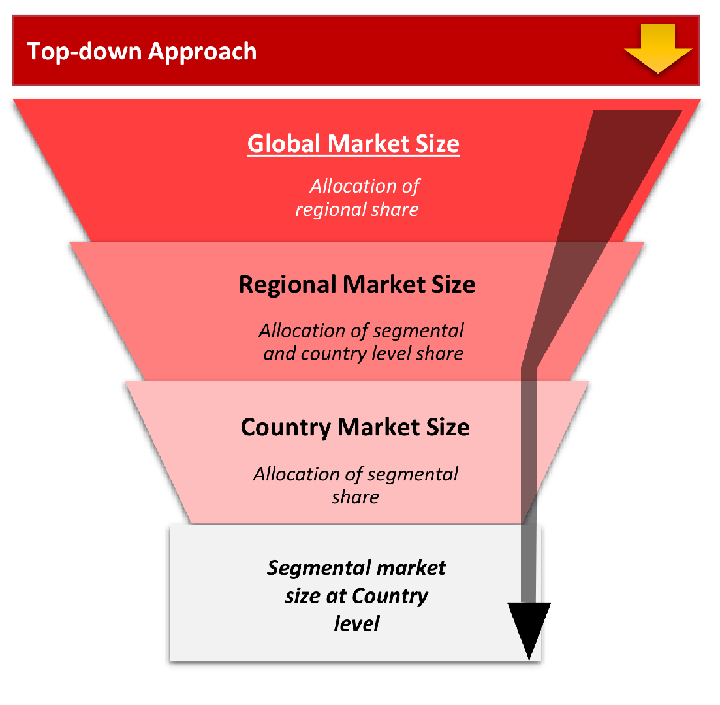
The top-down approach starts with the broadest possible market data and systematically narrows it down through a series of filters and assumptions to arrive at specific market segments or opportunities.
This method begins with the big picture and works downward to increasingly specific market slices.
TAM → SAM → SOM
Research Methods
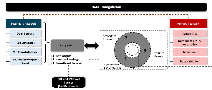
Desk / Secondary Research
While analysing the market, we extensively study secondary sources, directories, and databases to identify and collect information useful for this technical, market-oriented, and commercial report. Secondary sources that we utilize are not only the public sources, but it is a combination of Open Source, Associations, Paid Databases, MG Repository & Knowledgebase, and others.
- Company websites, annual reports, financial reports, broker reports, and investor presentations
- National government documents, statistical databases and reports
- News articles, press releases and web-casts specific to the companies operating in the market, Magazines, reports, and others
- We gather information from commercial data sources for deriving company specific data such as segmental revenue, share for geography, product revenue, and others
- Internal and external proprietary databases (industry-specific), relevant patent, and regulatory databases
- Governing Bodies, Government Organizations
- Relevant Authorities, Country-specific Associations for Industries
We also employ the model mapping approach to estimate the product level market data through the players' product portfolio
Primary Research
Primary research/ interviews is vital in analyzing the market. Most of the cases involves paid primary interviews. Primary sources include primary interviews through e-mail interactions, telephonic interviews, surveys as well as face-to-face interviews with the different stakeholders across the value chain including several industry experts.
| Type of Respondents | Number of Primaries |
|---|---|
| Tier 2/3 Suppliers | ~20 |
| Tier 1 Suppliers | ~25 |
| End-users | ~25 |
| Industry Expert/ Panel/ Consultant | ~30 |
| Total | ~100 |
MG Knowledgebase
• Repository of industry blog, newsletter and case studies
• Online platform covering detailed market reports, and company profiles
Forecasting Factors and Models
Forecasting Factors
- Historical Trends – Past market patterns, cycles, and major events that shaped how markets behave over time. Understanding past trends helps predict future behavior.
- Industry Factors – Specific characteristics of the industry like structure, regulations, and innovation cycles that affect market dynamics.
- Macroeconomic Factors – Economic conditions like GDP growth, inflation, and employment rates that affect how much money people have to spend.
- Demographic Factors – Population characteristics like age, income, and location that determine who can buy your product.
- Technology Factors – How quickly people adopt new technology and how much technology infrastructure exists.
- Regulatory Factors – Government rules, laws, and policies that can help or restrict market growth.
- Competitive Factors – Analyzing competition structure such as degree of competition and bargaining power of buyers and suppliers.
Forecasting Models / Techniques
Multiple Regression Analysis
- Identify and quantify factors that drive market changes
- Statistical modeling to establish relationships between market drivers and outcomes
Time Series Analysis – Seasonal Patterns
- Understand regular cyclical patterns in market demand
- Advanced statistical techniques to separate trend, seasonal, and irregular components
Time Series Analysis – Trend Analysis
- Identify underlying market growth patterns and momentum
- Statistical analysis of historical data to project future trends
Expert Opinion – Expert Interviews
- Gather deep industry insights and contextual understanding
- In-depth interviews with key industry stakeholders
Multi-Scenario Development
- Prepare for uncertainty by modeling different possible futures
- Creating optimistic, pessimistic, and most likely scenarios
Time Series Analysis – Moving Averages
- Sophisticated forecasting for complex time series data
- Auto-regressive integrated moving average models with seasonal components
Econometric Models
- Apply economic theory to market forecasting
- Sophisticated economic models that account for market interactions
Expert Opinion – Delphi Method
- Harness collective wisdom of industry experts
- Structured, multi-round expert consultation process
Monte Carlo Simulation
- Quantify uncertainty and probability distributions
- Thousands of simulations with varying input parameters
Research Analysis
Our research framework is built upon the fundamental principle of validating market intelligence from both demand and supply perspectives. This dual-sided approach ensures comprehensive market understanding and reduces the risk of single-source bias.
Demand-Side Analysis: We understand end-user/application behavior, preferences, and market needs along with the penetration of the product for specific application.
Supply-Side Analysis: We estimate overall market revenue, analyze the segmental share along with industry capacity, competitive landscape, and market structure.
Validation & Evaluation
Data triangulation is a validation technique that uses multiple methods, sources, or perspectives to examine the same research question, thereby increasing the credibility and reliability of research findings. In market research, triangulation serves as a quality assurance mechanism that helps identify and minimize bias, validate assumptions, and ensure accuracy in market estimates.
- Data Source Triangulation – Using multiple data sources to examine the same phenomenon
- Methodological Triangulation – Using multiple research methods to study the same research question
- Investigator Triangulation – Using multiple researchers or analysts to examine the same data
- Theoretical Triangulation – Using multiple theoretical perspectives to interpret the same data
Custom Market Research Services
We will customise the research for you, in case the report listed above does not meet your requirements.
Get 10% Free Customisation