Glass Wafer Carrier Market Size, Share & Trends Analysis Report by Product Type (Open Cassette Wafer Carriers, Closed Cassette Wafer Carriers, Front Opening Unified Pods (FOUPs), Single Wafer Carriers, Multi-Wafer Carriers, Custom Glass Wafer Carriers), Wafer Size, Material Type, Carrier Design, Functionality, Application and Geography (North America, Europe, Asia Pacific, Middle East, Africa and South America) – Global Industry Data, Trends and Forecasts, 2026–2035
|
|
|
Segmental Data Insights |
|
|
Demand Trends |
|
|
Competitive Landscape |
|
|
Strategic Development |
|
|
Future Outlook & Opportunities |
|
Glass Wafer Carrier Market Size, Share, and Growth
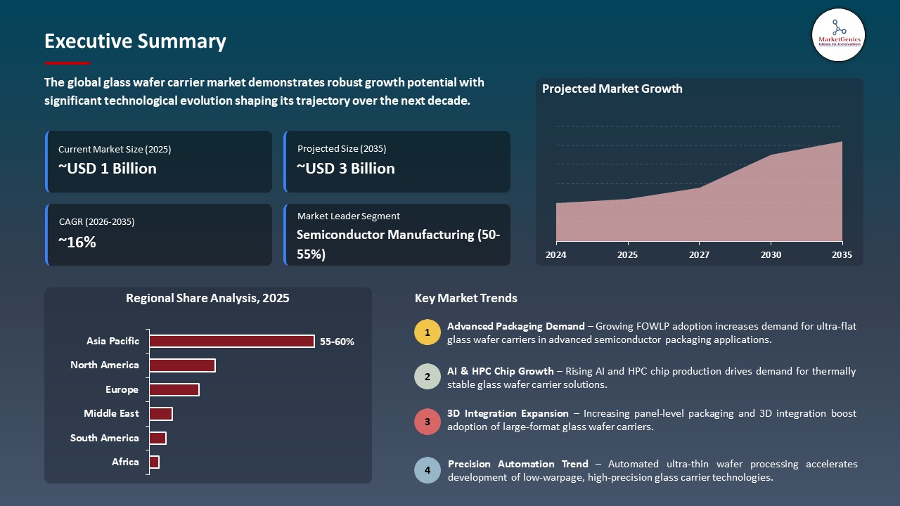
The global glass wafer carrier market is exhibiting strong growth, with an estimated value of USD 0.6 billion in 2025 and USD 2.8 billion by 2035, achieving a CAGR of 16.3%, during the forecast period. North America leads growth due to strong semiconductor manufacturing investments, CHIPS Act funding, advanced packaging adoption, presence of major fabs and equipment firms, and rapid expansion of domestic supply chains.
“The U.S. semiconductor industry's strength hinges on a reliable and advanced domestic supply chain of critical process chemistries and solutions,” said Entegris president and CEO Dave Reeder. “We are very proud that this state-of-the-art facility will be instrumental in realizing that vision for our customers, and building a more resilient semiconductor manufacturing ecosystem here in the U.S.”
The rapid expansion of advanced semiconductor packaging, including 2.5D/3D ICs and EUV lithography, is driving strong demand for ultra-precise, contamination-free glass wafer carrier solutions. For instance, Entegris, Inc. announced CHIPS Act–supported expansion of its Colorado Springs facility to increase advanced wafer carrier and FOUP production, reinforcing demand for high-performance carrier systems. This enhances yield, reduces contamination, and supports scalable advanced semiconductor manufacturing.
Moreover, the growing emphasis on supply chain localization and expansion of semiconductor manufacturing capacity is driving increased demand for advanced wafer carrier solutions. For instance, Gudeng Precision Industrial Co., Ltd. has been enhancing its EUV-compatible FOUP and advanced carrier solutions to support next-generation fabs, improving wafer protection and process efficiency in high-volume production environments. This strengthens manufacturing resilience, improves wafer safety, and enhances efficiency in high-volume semiconductor production.
Key adjacent opportunities for the global glass wafer carrier market include semiconductor advanced packaging substrates, wafer-level packaging (WLP) equipment, cleanroom automation systems, photomask handling solutions, and precision polymer/advanced materials. These segments benefit from growing chip miniaturization, EUV lithography adoption, and contamination-free manufacturing needs. These adjacencies expand value-chain integration, enhancing innovation and growth in semiconductor manufacturing ecosystems.
Glass Wafer Carrier Market Dynamics and Trends
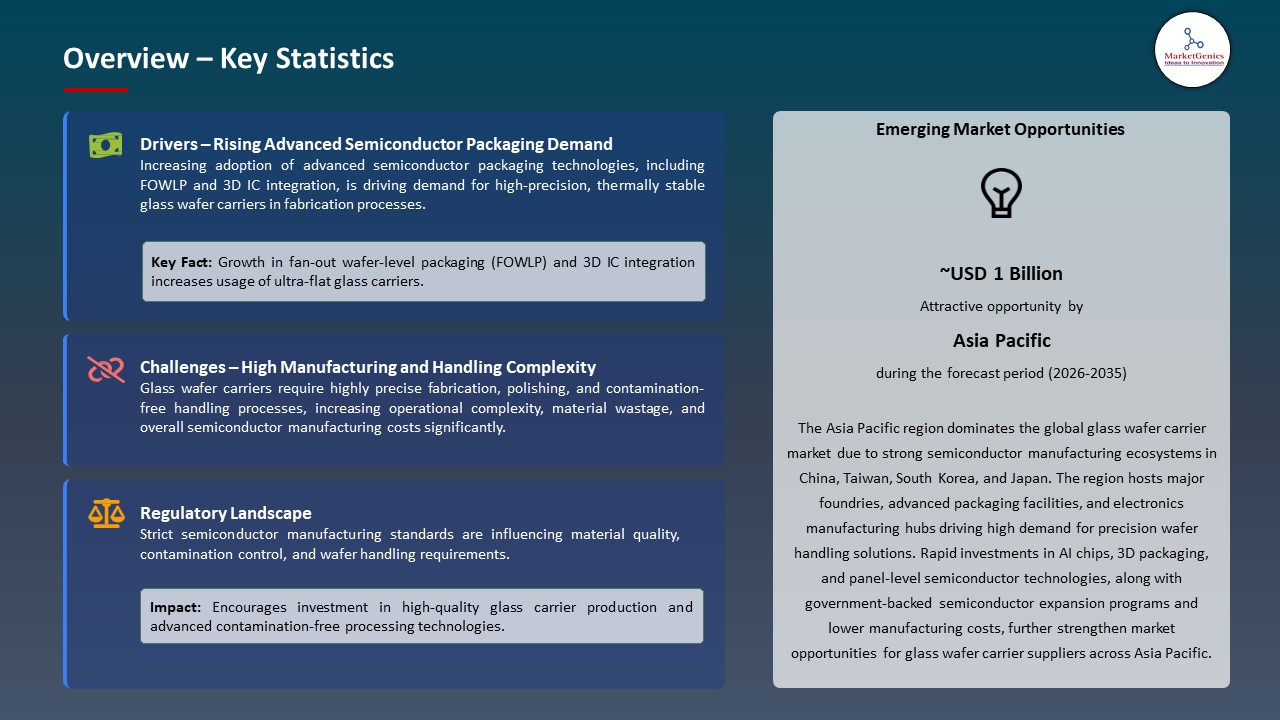
Driver: Accelerated Adoption of Glass Carriers in Advanced Semiconductor Packaging Ecosystems
- The glass wafer carrier market is seeing strong momentum, mainly because the shift toward glass-based substrates is speeding up in advanced semiconductor packaging use cases, like fan-out wafer-level packaging (FOWLP), panel-level packaging and AI-optimized chip architectures.
- For instance, Corning Incorporated’s official launch of “Advanced Packaging Carriers”, these are purpose engineered for semiconductor fan-out processes and also for high performance integrated circuit packaging. Corning has also said the glass carriers are designed to reduce wafer warpage during thinning and bonding operations, while at the same time improving mechanical stability, this validates the carriers for next generation semiconductor manufacturing environments.
- This faster adoption of glass substrates in advanced packaging is really sharpening demand visibility for glass wafer carriers, which keeps reinforcing their role in strengthening process stability, yield efficiency, and supporting scalable production of AI-driven semiconductor devices that perform really well.
Restraint: High Manufacturing Complexity and Elevated Production Cost Barriers
- The glass wafer carrier market is constrained by very complex, and also capital-intensive manufacturing stuff tied to precision glass processing. I mean, production really depends on advanced steps like fusion draw, chemical strengthening, ultra-fine polishing, plus really strict defect control just to get those ultra-flat surfaces needed for semiconductor packaging. Even small shifts in thickness, or surface quality can lead to wafer breakage, misalignment, or yield loss later on, especially during advanced processes like fan-out wafer-level packaging
- Additionally, making sure the thermal expansion matches silicon is another layer of engineering headache, so companies need specialized glass formulations with tightly controlled material properties. All these technical requirements push equipment costs up, stretch the production cycles longer than people expect, and they can lead to low first run yields which then makes it harder to scale in practice
- The high complexity and the heavy production costs reduce scalability, and that also keeps out many new players from entering the market.
Opportunity: Expansion of AI-driven Chiplet and Glass Core Substrate Integration
- The glass wafer carrier market is getting a strong lift from the growing shift toward AI driven chiplet architectures, and also glass core substrate integration, because semiconductors makers increasingly want materials that can help with high density interconnects, thermal steadiness, and really tight dimensional control. This change is basically pushing the demand for glass-based solutions in advanced packaging, especially in 3D stacking and mixed material chip setups where performance per square area is a big deal
- For instance, AGC’s official semiconductor solutions page notes that it’s Through Glass Via, TGV, substrates are made for 3D integration in advanced packaging use cases, including chiplet based systems, co-packaged optics, CPO, substrates, and RF devices. Additionally, in AGC investor disclosures, they say glass core substrates are expected to contribute a central role in next gen chiplet packaging frameworks, which is kind of where the momentum is coming from
- This wider adoption of AGC’s TGV and glass core substrate technologies is reinforcing the importance of glass wafer carriers for enabling scalable, high performance AI driven chiplet and advanced semiconductor packaging ecosystems.
Key Trend: Transition Toward Large-Format Panel-Level Glass Substrate Manufacturing
- The glass wafer carrier market is moving in a structural way toward large-format panel level glass substrate manufacturing, mostly because everyone is asking for higher packaging density, better cost efficiency and of course scalable production within advanced semiconductor ecosystems. As AI, HPC, and heterogeneous integration keep growing, manufacturers are looking at larger panel formats to get more die density and reduce the cost per chip.
- This change helps a lot with efficiency in fan out panel level packaging, plus it supports 2.5D/3D integration where stability and flatness are critical for yield, not to mention it also makes automation and throughput in high volume manufacturing run easier and faster.
- For instance, AGC and Corning both highlight scalable glass carrier and substrate development in their official semiconductor solutions portfolios, which shows broad industry agreement toward panel level architectures for those next generation packaging needs.
- Overall, the move toward panel level glass substrates is noticeably improving manufacturing efficiency, scalability, and cost competitiveness in advanced semiconductor packaging.
Glass Wafer Carrier Market Analysis and Segmental Data
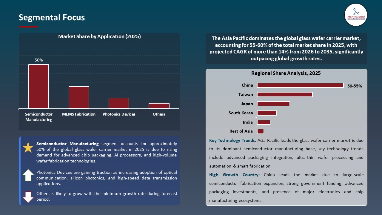
Semiconductor Manufacturing Dominate Global Glass Wafer Carrier Market
- The semiconductor manufacturing segment dominates the global glass wafer carrier market because advanced packaging procedures really rely on ultra-precise carrier substrates for chip handling, wafer thinning, and dimensional stability, not to mention all the practical needs in production. Semiconductor fabs more and more ask for glass carriers that can hold flatness, align with thermal expansion expectations, and also back yield-sensitive packaging workflows, even when lines are running fast.
- For instance, Nippon Electric Glass, which mentions on its semiconductor product page that its Glass Wafer for Supporting Semiconductors are high-precision carrier substrates used to support chips and other components in semiconductor packaging, with materials engineered to control thermal expansion behavior. That is, it’s basically positioned as a carefully tuned support platform rather than just a regular wafer part, and the wording is pretty direct.
- Overall, semiconductor manufacturing still stays as the core demand engine for glass wafer carriers, sustaining volume growth while reinforcing longer-term market stability, across multiple product generations.
Asia Pacific Leads Global Glass Wafer Carrier Market Demand
- Asia Pacific leads the glass wafer carrier market is driven by the concentration of leading semiconductor manufacturers and foundries. For instance, Samsung Electronics’ official semiconductor packaging announcements confirm expansion of advanced packaging lines for 2.5D and 3D integration, reinforcing demand for precision substrates in the region’s ecosystem.
- In addition, the aggressive scaling of memory and AI semiconductor production. For example, SK hynix has announced major investments to expand HBM production for AI applications. The company noted that advanced wafer-level packaging used in HBM manufacturing requires high-precision carrier substrates for process accuracy and yield improvement. This expansion is expected to increase demand for glass wafer carriers across high-volume semiconductor manufacturing in the Asia Pacific region.
- Asia Pacific’s leadership in advanced packaging and AI-driven memory expansion is significantly strengthening regional demand for glass wafer carriers, reinforcing its position as the global growth hub for the market.
Glass Wafer Carrier Market Ecosystem
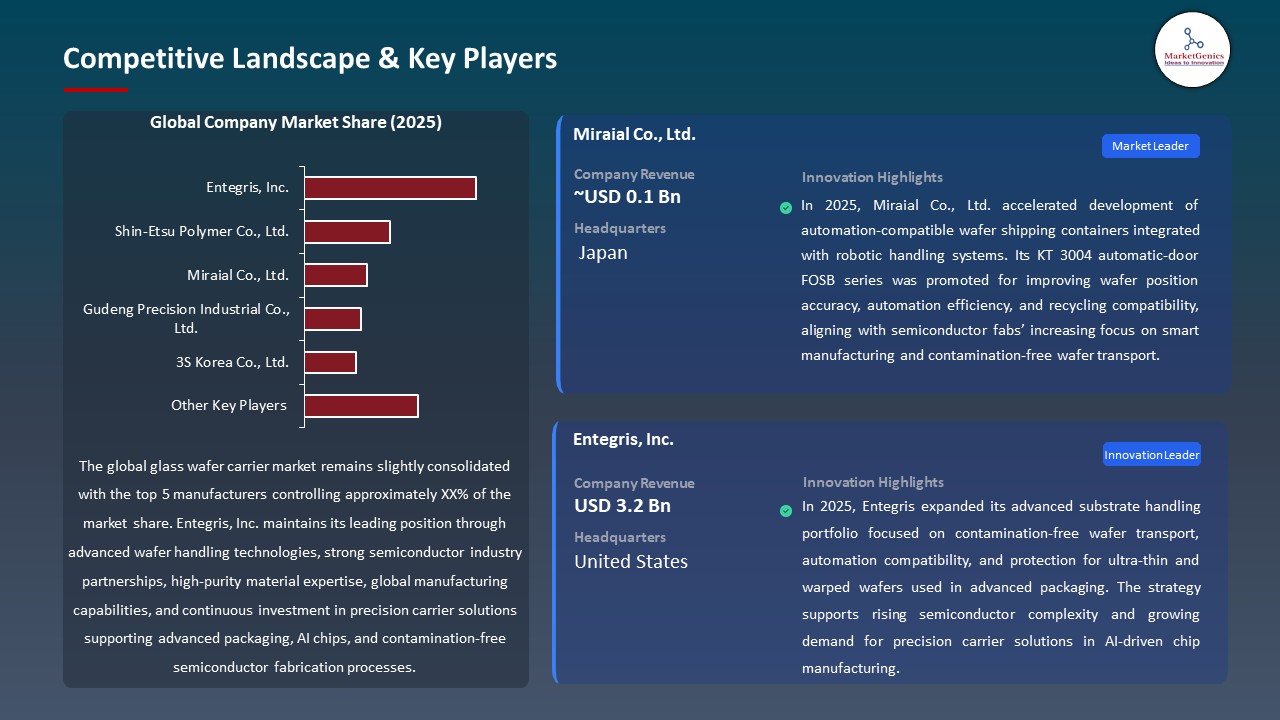
The global glass wafer carrier market is slightly consolidated, with leading players such as Entegris, Inc., Shin-Etsu Polymer Co., Ltd., Miraial Co., Ltd., Gudeng Precision Industrial Co., Ltd., and 3S Korea Co., Ltd. dominating through advanced material engineering, high-precision molding technologies, and contamination-free wafer handling solutions for semiconductor manufacturing. These companies leverage strong R&D capabilities and proprietary cleanroom-compatible carrier designs to maintain competitive leadership across advanced packaging ecosystems.
Key players are increasingly focusing on niche and specialized solutions such as ultra-flat glass wafer carriers, Front-Opening Unified Pods (FOUPs), and low-particle emission transport systems. For instance, Gudeng Precision emphasizes EUV-compatible FOUPs, while Miraial develops high-durability polymer and hybrid carriers designed for next-generation wafer thinning and handling efficiency.
These innovations collectively enhance wafer handling precision, reduce contamination risks, and improve yield rates in advanced semiconductor manufacturing, thereby strengthening process efficiency and supporting the scalability of next-generation packaging technologies.
Recent Development and Strategic Overview:
- In August 2024, WaferPro highlighted advanced wafer-level packaging (WLP) techniques including bonding, lithography, and thin-film processes. These capabilities support higher durability and signal integrity in miniaturized devices, indirectly reinforcing demand for glass wafer carriers used in handling fragile, ultra-thin wafers during complex semiconductor packaging steps.
- In June 2024, Entegris, Inc. announced up to $75 million CHIPS Act funding to expand its Colorado Springs manufacturing center, increasing Front-Opening Unified Pod (FOUP) and advanced wafer carrier production capacity. The strategy strengthens domestic semiconductor supply chains, supports advanced packaging growth, and reduces dependence on overseas wafer handling manufacturing ecosystems.
Report Scope
|
Detail |
|
|
Market Size in 2025 |
USD 0.6 Bn |
|
Market Forecast Value in 2035 |
USD 2.8 Bn |
|
Growth Rate (CAGR) |
16.3% |
|
Forecast Period |
2026 – 2035 |
|
Historical Data Available for |
2021 – 2024 |
|
Market Size Units |
US$ Billion for Value Thousand Units for Volume |
|
Report Format |
Electronic (PDF) + Excel |
|
North America |
Europe |
Asia Pacific |
Middle East |
Africa |
South America |
|
|
|
|
|
|
|
Companies Covered |
|||||
|
|
|
|
|
|
Glass Wafer Carrier Market Segmentation and Highlights
|
Segment |
Sub-segment |
|
Glass Wafer Carrier Market, By Product Type |
|
|
Glass Wafer Carrier Market, By Wafer Size |
|
|
Glass Wafer Carrier Market, By Material Type |
|
|
Glass Wafer Carrier Market, By Carrier Design |
|
|
Glass Wafer Carrier Market, By Functionality |
|
|
Glass Wafer Carrier Market, By Application |
|
Frequently Asked Questions
Table of Contents
- 1. Research Methodology and Assumptions
- 1.1. Definitions
- 1.2. Research Design and Approach
- 1.3. Data Collection Methods
- 1.4. Base Estimates and Calculations
- 1.5. Forecasting Models
- 1.5.1. Key Forecast Factors & Impact Analysis
- 1.6. Secondary Research
- 1.6.1. Open Sources
- 1.6.2. Paid Databases
- 1.6.3. Associations
- 1.7. Primary Research
- 1.7.1. Primary Sources
- 1.7.2. Primary Interviews with Stakeholders across Ecosystem
- 2. Executive Summary
- 2.1. Global Glass Wafer Carrier Market Outlook
- 2.1.1. Glass Wafer Carrier Market Size (Volume - Thousand Units and Value - US$ Bn), and Forecasts, 2021-2035
- 2.1.2. Compounded Annual Growth Rate Analysis
- 2.1.3. Growth Opportunity Analysis
- 2.1.4. Segmental Share Analysis
- 2.1.5. Geographical Share Analysis
- 2.2. Market Analysis and Facts
- 2.3. Supply-Demand Analysis
- 2.4. Competitive Benchmarking
- 2.5. Go-to- Market Strategy
- 2.5.1. Customer/ End-use Industry Assessment
- 2.5.2. Growth Opportunity Data, 2026-2035
- 2.5.2.1. Regional Data
- 2.5.2.2. Country Data
- 2.5.2.3. Segmental Data
- 2.5.3. Identification of Potential Market Spaces
- 2.5.4. GAP Analysis
- 2.5.5. Potential Attractive Price Points
- 2.5.6. Prevailing Market Risks & Challenges
- 2.5.7. Preferred Sales & Marketing Strategies
- 2.5.8. Key Recommendations and Analysis
- 2.5.9. A Way Forward
- 2.1. Global Glass Wafer Carrier Market Outlook
- 3. Industry Data and Premium Insights
- 3.1. Global Semiconductor & Electronics Industry Overview, 2025
- 3.1.1. Semiconductor & Electronics Ecosystem Analysis
- 3.1.2. Key Trends for Semiconductor & Electronics Industry
- 3.1.3. Regional Distribution for Semiconductor & Electronics Industry
- 3.2. Supplier Customer Data
- 3.3. Technology Roadmap and Developments
- 3.4. Trade Analysis
- 3.4.1. Import & Export Analysis, 2025
- 3.4.2. Top Importing Countries
- 3.4.3. Top Exporting Countries
- 3.5. Trump Tariff Impact Analysis
- 3.5.1. Manufacturer
- 3.5.1.1. Based on the component & Raw material
- 3.5.2. Supply Chain
- 3.5.3. End Consumer
- 3.5.1. Manufacturer
- 3.6. Raw Material Analysis
- 3.1. Global Semiconductor & Electronics Industry Overview, 2025
- 4. Market Overview
- 4.1. Market Dynamics
- 4.1.1. Drivers
- 4.1.1.1. Rising global semiconductor manufacturing and fab expansion demand
- 4.1.1.2. Growing adoption of advanced wafer-level and 3D semiconductor packaging
- 4.1.1.3. Increasing need for contamination-free, high-precision wafer handling solutions
- 4.1.2. Restraints
- 4.1.2.1. High manufacturing and raw material costs for precision glass carriers
- 4.1.2.2. Fragility and breakage risks associated with glass-based wafer carriers
- 4.1.1. Drivers
- 4.2. Key Trend Analysis
- 4.3. Regulatory Framework
- 4.3.1. Key Regulations, Norms, and Subsidies, by Key Countries
- 4.3.2. Tariffs and Standards
- 4.3.3. Impact Analysis of Regulations on the Market
- 4.4. Value Chain Analysis
- 4.4.1. Raw Material Suppliers
- 4.4.2. Glass Wafer Carrier Manufacturers
- 4.4.3. Foundry and OSAT
- 4.4.4. IDM and ODM
- 4.4.5. OEM and End Users
- 4.5. Porter’s Five Forces Analysis
- 4.6. PESTEL Analysis
- 4.7. Global Glass Wafer Carrier Market Demand
- 4.7.1. Historical Market Size – in Volume (Thousand Units) & Value (US$ Bn), 2020-2024
- 4.7.2. Current and Future Market Size – in Volume (Thousand Units) & Value (US$ Bn), 2026–2035
- 4.7.2.1. Y-o-Y Growth Trends
- 4.7.2.2. Absolute $ Opportunity Assessment
- 4.1. Market Dynamics
- 5. Competition Landscape
- 5.1. Competition structure
- 5.1.1. Fragmented v/s consolidated
- 5.2. Company Share Analysis, 2025
- 5.2.1. Global Company Market Share
- 5.2.2. By Region
- 5.2.2.1. North America
- 5.2.2.2. Europe
- 5.2.2.3. Asia Pacific
- 5.2.2.4. Middle East
- 5.2.2.5. Africa
- 5.2.2.6. South America
- 5.3. Product Comparison Matrix
- 5.3.1. Specifications
- 5.3.2. Market Positioning
- 5.3.3. Pricing
- 5.1. Competition structure
- 6. Global Glass Wafer Carrier Market Analysis, by Product Type
- 6.1. Key Segment Analysis
- 6.2. Glass Wafer Carrier Market Size (Volume - Thousand Units and Value - US$ Bn), Analysis, and Forecasts, by Product Type, 2021-2035
- 6.2.1. Open Cassette Wafer Carriers
- 6.2.2. Closed Cassette Wafer Carriers
- 6.2.3. Front Opening Unified Pods (FOUPs)
- 6.2.4. Single Wafer Carriers
- 6.2.5. Multi-Wafer Carriers
- 6.2.6. Custom Glass Wafer Carriers
- 7. Global Glass Wafer Carrier Market Analysis, by Wafer Size
- 7.1. Key Segment Analysis
- 7.2. Glass Wafer Carrier Market Size (Volume - Thousand Units and Value - US$ Bn), Analysis, and Forecasts, by Wafer Size, 2021-2035
- 7.2.1. Up to 100 mm
- 7.2.2. 100 mm–200 mm
- 7.2.3. 200 mm–300 mm
- 7.2.4. Above 300 mm
- 8. Global Glass Wafer Carrier Market Analysis, by Material Type
- 8.1. Key Segment Analysis
- 8.2. Glass Wafer Carrier Market Size (Volume - Thousand Units and Value - US$ Bn), Analysis, and Forecasts, by Material Type, 2021-2035
- 8.2.1. Quartz Glass
- 8.2.2. Borosilicate Glass
- 8.2.3. Tempered Glass
- 8.2.4. Fused Silica Glass
- 8.2.5. Specialty Coated Glass
- 9. Global Glass Wafer Carrier Market Analysis, by Carrier Design
- 9.1. Key Segment Analysis
- 9.2. Glass Wafer Carrier Market Size (Volume - Thousand Units and Value - US$ Bn), Analysis, and Forecasts, by Carrier Design, 2021-2035
- 9.2.1. Horizontal Wafer Carriers
- 9.2.2. Vertical Wafer Carriers
- 9.2.3. Stackable Wafer Carriers
- 9.2.4. Automated Handling-Compatible Carriers
- 9.2.5. Others
- 10. Global Glass Wafer Carrier Market Analysis, by Functionality
- 10.1. Key Segment Analysis
- 10.2. Glass Wafer Carrier Market Size (Volume - Thousand Units and Value - US$ Bn), Analysis, and Forecasts, by Functionality, 2021-2035
- 10.2.1. Anti-Static Carriers
- 10.2.2. High-Temperature Resistant Carriers
- 10.2.3. Chemical Resistant Carriers
- 10.2.4. Scratch-Protected Carriers
- 10.2.5. Precision Alignment Carriers
- 10.2.6. Others
- 11. Global Glass Wafer Carrier Market Analysis, by Application
- 11.1. Key Segment Analysis
- 11.2. Glass Wafer Carrier Market Size (Volume - Thousand Units and Value - US$ Bn), Analysis, and Forecasts, by Application, 2021-2035
- 11.2.1. Semiconductor Manufacturing
- 11.2.2. MEMS Fabrication
- 11.2.3. Photonics Devices
- 11.2.4. LED Manufacturing
- 11.2.5. Solar Cell Processing
- 11.2.6. Advanced Packaging
- 11.2.7. Others
- 12. Global Glass Wafer Carrier Market Analysis, by Region
- 12.1. Key Findings
- 12.2. Glass Wafer Carrier Market Size (Volume - Thousand Units and Value - US$ Bn), Analysis, and Forecasts, by Region, 2021-2035
- 12.2.1. North America
- 12.2.2. Europe
- 12.2.3. Asia Pacific
- 12.2.4. Middle East
- 12.2.5. Africa
- 12.2.6. South America
- 13. North America Glass Wafer Carrier Market Analysis
- 13.1. Key Segment Analysis
- 13.2. Regional Snapshot
- 13.3. North America Glass Wafer Carrier Market Size (Volume - Thousand Units and Value - US$ Bn), Analysis, and Forecasts, 2021-2035
- 13.3.1. Product Type
- 13.3.2. Wafer Size
- 13.3.3. Material Type
- 13.3.4. Carrier Design
- 13.3.5. Functionality
- 13.3.6. Application
- 13.3.7. Country
- 13.3.7.1. USA
- 13.3.7.2. Canada
- 13.3.7.3. Mexico
- 13.4. USA Glass Wafer Carrier Market
- 13.4.1. Country Segmental Analysis
- 13.4.2. Product Type
- 13.4.3. Wafer Size
- 13.4.4. Material Type
- 13.4.5. Carrier Design
- 13.4.6. Functionality
- 13.4.7. Application
- 13.5. Canada Glass Wafer Carrier Market
- 13.5.1. Country Segmental Analysis
- 13.5.2. Product Type
- 13.5.3. Wafer Size
- 13.5.4. Material Type
- 13.5.5. Carrier Design
- 13.5.6. Functionality
- 13.5.7. Application
- 13.6. Mexico Glass Wafer Carrier Market
- 13.6.1. Country Segmental Analysis
- 13.6.2. Product Type
- 13.6.3. Wafer Size
- 13.6.4. Material Type
- 13.6.5. Carrier Design
- 13.6.6. Functionality
- 13.6.7. Application
- 14. Europe Glass Wafer Carrier Market Analysis
- 14.1. Key Segment Analysis
- 14.2. Regional Snapshot
- 14.3. Europe Glass Wafer Carrier Market Size (Volume - Thousand Units and Value - US$ Bn), Analysis, and Forecasts, 2021-2035
- 14.3.1. Product Type
- 14.3.2. Wafer Size
- 14.3.3. Material Type
- 14.3.4. Carrier Design
- 14.3.5. Functionality
- 14.3.6. Application
- 14.3.7. Country
- 14.3.7.1. Germany
- 14.3.7.2. United Kingdom
- 14.3.7.3. France
- 14.3.7.4. Italy
- 14.3.7.5. Spain
- 14.3.7.6. Netherlands
- 14.3.7.7. Nordic Countries
- 14.3.7.8. Poland
- 14.3.7.9. Russia & CIS
- 14.3.7.10. Rest of Europe
- 14.4. Germany Glass Wafer Carrier Market
- 14.4.1. Country Segmental Analysis
- 14.4.2. Product Type
- 14.4.3. Wafer Size
- 14.4.4. Material Type
- 14.4.5. Carrier Design
- 14.4.6. Functionality
- 14.4.7. Application
- 14.5. United Kingdom Glass Wafer Carrier Market
- 14.5.1. Country Segmental Analysis
- 14.5.2. Product Type
- 14.5.3. Wafer Size
- 14.5.4. Material Type
- 14.5.5. Carrier Design
- 14.5.6. Functionality
- 14.5.7. Application
- 14.6. France Glass Wafer Carrier Market
- 14.6.1. Country Segmental Analysis
- 14.6.2. Product Type
- 14.6.3. Wafer Size
- 14.6.4. Material Type
- 14.6.5. Carrier Design
- 14.6.6. Functionality
- 14.6.7. Application
- 14.7. Italy Glass Wafer Carrier Market
- 14.7.1. Country Segmental Analysis
- 14.7.2. Product Type
- 14.7.3. Wafer Size
- 14.7.4. Material Type
- 14.7.5. Carrier Design
- 14.7.6. Functionality
- 14.7.7. Application
- 14.8. Spain Glass Wafer Carrier Market
- 14.8.1. Country Segmental Analysis
- 14.8.2. Product Type
- 14.8.3. Wafer Size
- 14.8.4. Material Type
- 14.8.5. Carrier Design
- 14.8.6. Functionality
- 14.8.7. Application
- 14.9. Netherlands Glass Wafer Carrier Market
- 14.9.1. Country Segmental Analysis
- 14.9.2. Product Type
- 14.9.3. Wafer Size
- 14.9.4. Material Type
- 14.9.5. Carrier Design
- 14.9.6. Functionality
- 14.9.7. Application
- 14.10. Nordic Countries Glass Wafer Carrier Market
- 14.10.1. Country Segmental Analysis
- 14.10.2. Product Type
- 14.10.3. Wafer Size
- 14.10.4. Material Type
- 14.10.5. Carrier Design
- 14.10.6. Functionality
- 14.10.7. Application
- 14.11. Poland Glass Wafer Carrier Market
- 14.11.1. Country Segmental Analysis
- 14.11.2. Product Type
- 14.11.3. Wafer Size
- 14.11.4. Material Type
- 14.11.5. Carrier Design
- 14.11.6. Functionality
- 14.11.7. Application
- 14.12. Russia & CIS Glass Wafer Carrier Market
- 14.12.1. Country Segmental Analysis
- 14.12.2. Product Type
- 14.12.3. Wafer Size
- 14.12.4. Material Type
- 14.12.5. Carrier Design
- 14.12.6. Functionality
- 14.12.7. Application
- 14.13. Rest of Europe Glass Wafer Carrier Market
- 14.13.1. Country Segmental Analysis
- 14.13.2. Product Type
- 14.13.3. Wafer Size
- 14.13.4. Material Type
- 14.13.5. Carrier Design
- 14.13.6. Functionality
- 14.13.7. Application
- 15. Asia Pacific Glass Wafer Carrier Market Analysis
- 15.1. Key Segment Analysis
- 15.2. Regional Snapshot
- 15.3. Asia Pacific Glass Wafer Carrier Market Size (Volume - Thousand Units and Value - US$ Bn), Analysis, and Forecasts, 2021-2035
- 15.3.1. Product Type
- 15.3.2. Wafer Size
- 15.3.3. Material Type
- 15.3.4. Carrier Design
- 15.3.5. Functionality
- 15.3.6. Application
- 15.3.7. Country
- 15.3.7.1. China
- 15.3.7.2. India
- 15.3.7.3. Japan
- 15.3.7.4. South Korea
- 15.3.7.5. Australia and New Zealand
- 15.3.7.6. Indonesia
- 15.3.7.7. Malaysia
- 15.3.7.8. Thailand
- 15.3.7.9. Vietnam
- 15.3.7.10. Rest of Asia Pacific
- 15.4. China Glass Wafer Carrier Market
- 15.4.1. Country Segmental Analysis
- 15.4.2. Product Type
- 15.4.3. Wafer Size
- 15.4.4. Material Type
- 15.4.5. Carrier Design
- 15.4.6. Functionality
- 15.4.7. Application
- 15.5. India Glass Wafer Carrier Market
- 15.5.1. Country Segmental Analysis
- 15.5.2. Product Type
- 15.5.3. Wafer Size
- 15.5.4. Material Type
- 15.5.5. Carrier Design
- 15.5.6. Functionality
- 15.5.7. Application
- 15.6. Japan Glass Wafer Carrier Market
- 15.6.1. Country Segmental Analysis
- 15.6.2. Product Type
- 15.6.3. Wafer Size
- 15.6.4. Material Type
- 15.6.5. Carrier Design
- 15.6.6. Functionality
- 15.6.7. Application
- 15.7. South Korea Glass Wafer Carrier Market
- 15.7.1. Country Segmental Analysis
- 15.7.2. Product Type
- 15.7.3. Wafer Size
- 15.7.4. Material Type
- 15.7.5. Carrier Design
- 15.7.6. Functionality
- 15.7.7. Application
- 15.8. Australia and New Zealand Glass Wafer Carrier Market
- 15.8.1. Country Segmental Analysis
- 15.8.2. Product Type
- 15.8.3. Wafer Size
- 15.8.4. Material Type
- 15.8.5. Carrier Design
- 15.8.6. Functionality
- 15.8.7. Application
- 15.9. Indonesia Glass Wafer Carrier Market
- 15.9.1. Country Segmental Analysis
- 15.9.2. Product Type
- 15.9.3. Wafer Size
- 15.9.4. Material Type
- 15.9.5. Carrier Design
- 15.9.6. Functionality
- 15.9.7. Application
- 15.10. Malaysia Glass Wafer Carrier Market
- 15.10.1. Country Segmental Analysis
- 15.10.2. Product Type
- 15.10.3. Wafer Size
- 15.10.4. Material Type
- 15.10.5. Carrier Design
- 15.10.6. Functionality
- 15.10.7. Application
- 15.11. Thailand Glass Wafer Carrier Market
- 15.11.1. Country Segmental Analysis
- 15.11.2. Product Type
- 15.11.3. Wafer Size
- 15.11.4. Material Type
- 15.11.5. Carrier Design
- 15.11.6. Functionality
- 15.11.7. Application
- 15.12. Vietnam Glass Wafer Carrier Market
- 15.12.1. Country Segmental Analysis
- 15.12.2. Product Type
- 15.12.3. Wafer Size
- 15.12.4. Material Type
- 15.12.5. Carrier Design
- 15.12.6. Functionality
- 15.12.7. Application
- 15.13. Rest of Asia Pacific Glass Wafer Carrier Market
- 15.13.1. Country Segmental Analysis
- 15.13.2. Product Type
- 15.13.3. Wafer Size
- 15.13.4. Material Type
- 15.13.5. Carrier Design
- 15.13.6. Functionality
- 15.13.7. Application
- 16. Middle East Glass Wafer Carrier Market Analysis
- 16.1. Key Segment Analysis
- 16.2. Regional Snapshot
- 16.3. Middle East Glass Wafer Carrier Market Size (Volume - Thousand Units and Value - US$ Bn), Analysis, and Forecasts, 2021-2035
- 16.3.1. Product Type
- 16.3.2. Wafer Size
- 16.3.3. Material Type
- 16.3.4. Carrier Design
- 16.3.5. Functionality
- 16.3.6. Application
- 16.3.7. Country
- 16.3.7.1. Turkey
- 16.3.7.2. UAE
- 16.3.7.3. Saudi Arabia
- 16.3.7.4. Israel
- 16.3.7.5. Rest of Middle East
- 16.4. Turkey Glass Wafer Carrier Market
- 16.4.1. Country Segmental Analysis
- 16.4.2. Product Type
- 16.4.3. Wafer Size
- 16.4.4. Material Type
- 16.4.5. Carrier Design
- 16.4.6. Functionality
- 16.4.7. Application
- 16.5. UAE Glass Wafer Carrier Market
- 16.5.1. Country Segmental Analysis
- 16.5.2. Product Type
- 16.5.3. Wafer Size
- 16.5.4. Material Type
- 16.5.5. Carrier Design
- 16.5.6. Functionality
- 16.5.7. Application
- 16.6. Saudi Arabia Glass Wafer Carrier Market
- 16.6.1. Country Segmental Analysis
- 16.6.2. Product Type
- 16.6.3. Wafer Size
- 16.6.4. Material Type
- 16.6.5. Carrier Design
- 16.6.6. Functionality
- 16.6.7. Application
- 16.7. Israel Glass Wafer Carrier Market
- 16.7.1. Country Segmental Analysis
- 16.7.2. Product Type
- 16.7.3. Wafer Size
- 16.7.4. Material Type
- 16.7.5. Carrier Design
- 16.7.6. Functionality
- 16.7.7. Application
- 16.8. Rest of Middle East Glass Wafer Carrier Market
- 16.8.1. Country Segmental Analysis
- 16.8.2. Product Type
- 16.8.3. Wafer Size
- 16.8.4. Material Type
- 16.8.5. Carrier Design
- 16.8.6. Functionality
- 16.8.7. Application
- 17. Africa Glass Wafer Carrier Market Analysis
- 17.1. Key Segment Analysis
- 17.2. Regional Snapshot
- 17.3. Africa Glass Wafer Carrier Market Size (Volume - Thousand Units and Value - US$ Bn), Analysis, and Forecasts, 2021-2035
- 17.3.1. Product Type
- 17.3.2. Wafer Size
- 17.3.3. Material Type
- 17.3.4. Carrier Design
- 17.3.5. Functionality
- 17.3.6. Application
- 17.3.7. Country
- 17.3.7.1. South Africa
- 17.3.7.2. Egypt
- 17.3.7.3. Nigeria
- 17.3.7.4. Algeria
- 17.3.7.5. Rest of Africa
- 17.4. South Africa Glass Wafer Carrier Market
- 17.4.1. Country Segmental Analysis
- 17.4.2. Product Type
- 17.4.3. Wafer Size
- 17.4.4. Material Type
- 17.4.5. Carrier Design
- 17.4.6. Functionality
- 17.4.7. Application
- 17.5. Egypt Glass Wafer Carrier Market
- 17.5.1. Country Segmental Analysis
- 17.5.2. Product Type
- 17.5.3. Wafer Size
- 17.5.4. Material Type
- 17.5.5. Carrier Design
- 17.5.6. Functionality
- 17.5.7. Application
- 17.6. Nigeria Glass Wafer Carrier Market
- 17.6.1. Country Segmental Analysis
- 17.6.2. Product Type
- 17.6.3. Wafer Size
- 17.6.4. Material Type
- 17.6.5. Carrier Design
- 17.6.6. Functionality
- 17.6.7. Application
- 17.7. Algeria Glass Wafer Carrier Market
- 17.7.1. Country Segmental Analysis
- 17.7.2. Product Type
- 17.7.3. Wafer Size
- 17.7.4. Material Type
- 17.7.5. Carrier Design
- 17.7.6. Functionality
- 17.7.7. Application
- 17.8. Rest of Africa Glass Wafer Carrier Market
- 17.8.1. Country Segmental Analysis
- 17.8.2. Product Type
- 17.8.3. Wafer Size
- 17.8.4. Material Type
- 17.8.5. Carrier Design
- 17.8.6. Functionality
- 17.8.7. Application
- 18. South America Glass Wafer Carrier Market Analysis
- 18.1. Key Segment Analysis
- 18.2. Regional Snapshot
- 18.3. South America Glass Wafer Carrier Market Size (Volume - Thousand Units and Value - US$ Bn), Analysis, and Forecasts, 2021-2035
- 18.3.1. Product Type
- 18.3.2. Wafer Size
- 18.3.3. Material Type
- 18.3.4. Carrier Design
- 18.3.5. Functionality
- 18.3.6. Application
- 18.3.7. Country
- 18.3.7.1. Brazil
- 18.3.7.2. Argentina
- 18.3.7.3. Rest of South America
- 18.4. Brazil Glass Wafer Carrier Market
- 18.4.1. Country Segmental Analysis
- 18.4.2. Product Type
- 18.4.3. Wafer Size
- 18.4.4. Material Type
- 18.4.5. Carrier Design
- 18.4.6. Functionality
- 18.4.7. Application
- 18.5. Argentina Glass Wafer Carrier Market
- 18.5.1. Country Segmental Analysis
- 18.5.2. Product Type
- 18.5.3. Wafer Size
- 18.5.4. Material Type
- 18.5.5. Carrier Design
- 18.5.6. Functionality
- 18.5.7. Application
- 18.6. Rest of South America Glass Wafer Carrier Market
- 18.6.1. Country Segmental Analysis
- 18.6.2. Product Type
- 18.6.3. Wafer Size
- 18.6.4. Material Type
- 18.6.5. Carrier Design
- 18.6.6. Functionality
- 18.6.7. Application
- 19. Key Players/ Company Profile
- 19.1. 3S Korea Co., Ltd.
- 19.1.1. Company Details/ Overview
- 19.1.2. Company Financials
- 19.1.3. Key Customers and Competitors
- 19.1.4. Business/ Industry Portfolio
- 19.1.5. Product Portfolio/ Specification Details
- 19.1.6. Pricing Data
- 19.1.7. Strategic Overview
- 19.1.8. Recent Developments
- 19.2. Advance International Corp.
- 19.3. Brooks Automation, Inc.
- 19.4. Chung King Enterprise Co., Ltd.
- 19.5. Clean Room Devices, Inc.
- 19.6. Daewon Semiconductor Packaging Industrial Co., Ltd.
- 19.7. Dainichi Shoji K.K.
- 19.8. Entegris, Inc.
- 19.9. ePAK International, Inc.
- 19.10. E-SUN Precision Industrial Co., Ltd.
- 19.11. Gudeng Precision Industrial Co., Ltd.
- 19.12. H-Square Corporation
- 19.13. Kostat, Inc.
- 19.14. Miraial Co., Ltd.
- 19.15. Pozzetta Products, Inc.
- 19.16. Shin-Etsu Polymer Co., Ltd.
- 19.17. Silicon Valley Microelectronics, Inc.
- 19.18. Ted Pella, Inc.
- 19.19. Toyo Adtec Inc.
- 19.20. WaferPro LLC
- 19.21. Other Key Players
- 19.1. 3S Korea Co., Ltd.
Note* - This is just tentative list of players. While providing the report, we will cover more number of players based on their revenue and share for each geography
Research Design
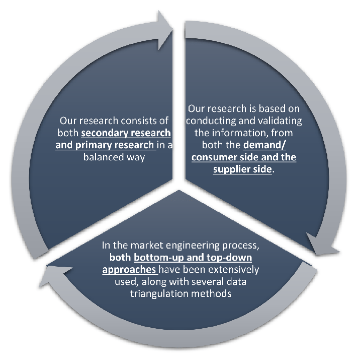
Our research design integrates both demand-side and supply-side analysis through a balanced combination of primary and secondary research methodologies. By utilizing both bottom-up and top-down approaches alongside rigorous data triangulation methods, we deliver robust market intelligence that supports strategic decision-making.
MarketGenics' comprehensive research design framework ensures the delivery of accurate, reliable, and actionable market intelligence. Through the integration of multiple research approaches, rigorous validation processes, and expert analysis, we provide our clients with the insights needed to make informed strategic decisions and capitalize on market opportunities.
MarketGenics leverages a dedicated industry panel of experts and a comprehensive suite of paid databases to effectively collect, consolidate, and analyze market intelligence.
Our approach has consistently proven to be reliable and effective in generating accurate market insights, identifying key industry trends, and uncovering emerging business opportunities.
Through both primary and secondary research, we capture and analyze critical company-level data such as manufacturing footprints, including technical centers, R&D facilities, sales offices, and headquarters.
Our expert panel further enhances our ability to estimate market size for specific brands based on validated field-level intelligence.
Our data mining techniques incorporate both parametric and non-parametric methods, allowing for structured data collection, sorting, processing, and cleaning.
Demand projections are derived from large-scale data sets analyzed through proprietary algorithms, culminating in robust and reliable market sizing.
Research Approach
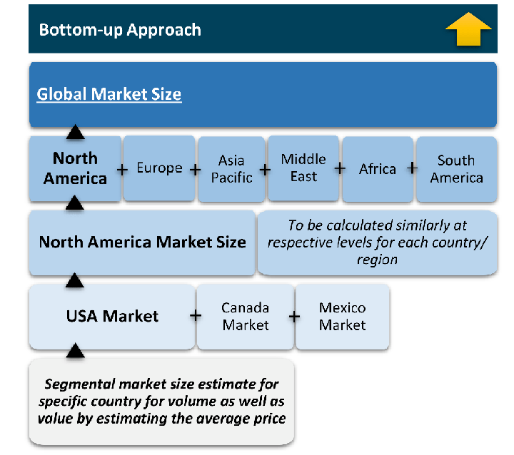
The bottom-up approach builds market estimates by starting with the smallest addressable market units and systematically aggregating them to create comprehensive market size projections.
This method begins with specific, granular data points and builds upward to create the complete market landscape.
Customer Analysis → Segmental Analysis → Geographical Analysis
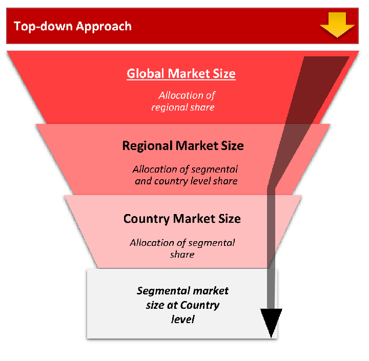
The top-down approach starts with the broadest possible market data and systematically narrows it down through a series of filters and assumptions to arrive at specific market segments or opportunities.
This method begins with the big picture and works downward to increasingly specific market slices.
TAM → SAM → SOM
Research Methods
Desk / Secondary Research
While analysing the market, we extensively study secondary sources, directories, and databases to identify and collect information useful for this technical, market-oriented, and commercial report. Secondary sources that we utilize are not only the public sources, but it is a combination of Open Source, Associations, Paid Databases, MG Repository & Knowledgebase, and others.
- Company websites, annual reports, financial reports, broker reports, and investor presentations
- National government documents, statistical databases and reports
- News articles, press releases and web-casts specific to the companies operating in the market, Magazines, reports, and others
- We gather information from commercial data sources for deriving company specific data such as segmental revenue, share for geography, product revenue, and others
- Internal and external proprietary databases (industry-specific), relevant patent, and regulatory databases
- Governing Bodies, Government Organizations
- Relevant Authorities, Country-specific Associations for Industries
We also employ the model mapping approach to estimate the product level market data through the players' product portfolio
Primary Research
Primary research/ interviews is vital in analyzing the market. Most of the cases involves paid primary interviews. Primary sources include primary interviews through e-mail interactions, telephonic interviews, surveys as well as face-to-face interviews with the different stakeholders across the value chain including several industry experts.
| Type of Respondents | Number of Primaries |
|---|---|
| Tier 2/3 Suppliers | ~20 |
| Tier 1 Suppliers | ~25 |
| End-users | ~25 |
| Industry Expert/ Panel/ Consultant | ~30 |
| Total | ~100 |
MG Knowledgebase
• Repository of industry blog, newsletter and case studies
• Online platform covering detailed market reports, and company profiles
Forecasting Factors and Models
Forecasting Factors
- Historical Trends – Past market patterns, cycles, and major events that shaped how markets behave over time. Understanding past trends helps predict future behavior.
- Industry Factors – Specific characteristics of the industry like structure, regulations, and innovation cycles that affect market dynamics.
- Macroeconomic Factors – Economic conditions like GDP growth, inflation, and employment rates that affect how much money people have to spend.
- Demographic Factors – Population characteristics like age, income, and location that determine who can buy your product.
- Technology Factors – How quickly people adopt new technology and how much technology infrastructure exists.
- Regulatory Factors – Government rules, laws, and policies that can help or restrict market growth.
- Competitive Factors – Analyzing competition structure such as degree of competition and bargaining power of buyers and suppliers.
Forecasting Models / Techniques
Multiple Regression Analysis
- Identify and quantify factors that drive market changes
- Statistical modeling to establish relationships between market drivers and outcomes
Time Series Analysis – Seasonal Patterns
- Understand regular cyclical patterns in market demand
- Advanced statistical techniques to separate trend, seasonal, and irregular components
Time Series Analysis – Trend Analysis
- Identify underlying market growth patterns and momentum
- Statistical analysis of historical data to project future trends
Expert Opinion – Expert Interviews
- Gather deep industry insights and contextual understanding
- In-depth interviews with key industry stakeholders
Multi-Scenario Development
- Prepare for uncertainty by modeling different possible futures
- Creating optimistic, pessimistic, and most likely scenarios
Time Series Analysis – Moving Averages
- Sophisticated forecasting for complex time series data
- Auto-regressive integrated moving average models with seasonal components
Econometric Models
- Apply economic theory to market forecasting
- Sophisticated economic models that account for market interactions
Expert Opinion – Delphi Method
- Harness collective wisdom of industry experts
- Structured, multi-round expert consultation process
Monte Carlo Simulation
- Quantify uncertainty and probability distributions
- Thousands of simulations with varying input parameters
Research Analysis
Our research framework is built upon the fundamental principle of validating market intelligence from both demand and supply perspectives. This dual-sided approach ensures comprehensive market understanding and reduces the risk of single-source bias.
Demand-Side Analysis: We understand end-user/application behavior, preferences, and market needs along with the penetration of the product for specific application.
Supply-Side Analysis: We estimate overall market revenue, analyze the segmental share along with industry capacity, competitive landscape, and market structure.
Validation & Evaluation
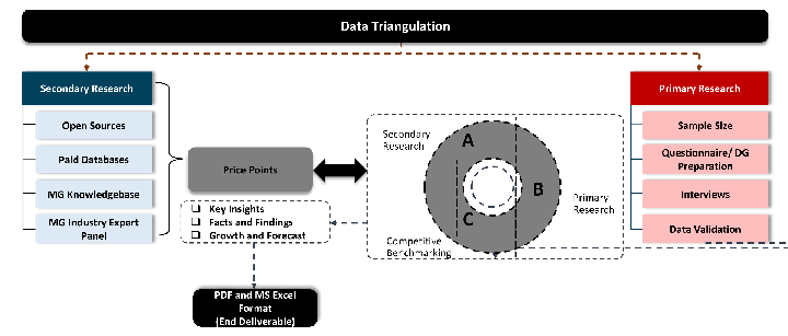
Data triangulation is a validation technique that uses multiple methods, sources, or perspectives to examine the same research question, thereby increasing the credibility and reliability of research findings. In market research, triangulation serves as a quality assurance mechanism that helps identify and minimize bias, validate assumptions, and ensure accuracy in market estimates.
- Data Source Triangulation – Using multiple data sources to examine the same phenomenon
- Methodological Triangulation – Using multiple research methods to study the same research question
- Investigator Triangulation – Using multiple researchers or analysts to examine the same data
- Theoretical Triangulation – Using multiple theoretical perspectives to interpret the same data
Custom Market Research Services
We will customise the research for you, in case the report listed above does not meet your requirements.
Get 10% Free Customisation