Fan-Out Wafer Level Packaging (FOWLP) Market Size, Share & Trends Analysis Report by Packaging Technology (Chip-First FOWLP, Chip-Last FOWLP, Embedded Die Fan-Out Packaging, Integrated Fan-Out Packaging, Hybrid Fan-Out Packaging), Carrier Type, Number of I/O Pins, Technology Node, Wafer Size, Integration Level, Application, End Users, and Geography (North America, Europe, Asia Pacific, Middle East, Africa, and South America) – Global Industry Data, Trends, and Forecasts, 2026–2035
|
|
|
Segmental Data Insights |
|
|
Demand Trends |
|
|
Competitive Landscape |
|
|
Strategic Development |
|
|
Future Outlook & Opportunities |
|
Fan-Out Wafer Level Packaging (FOWLP) Market Size, Share, and Growth
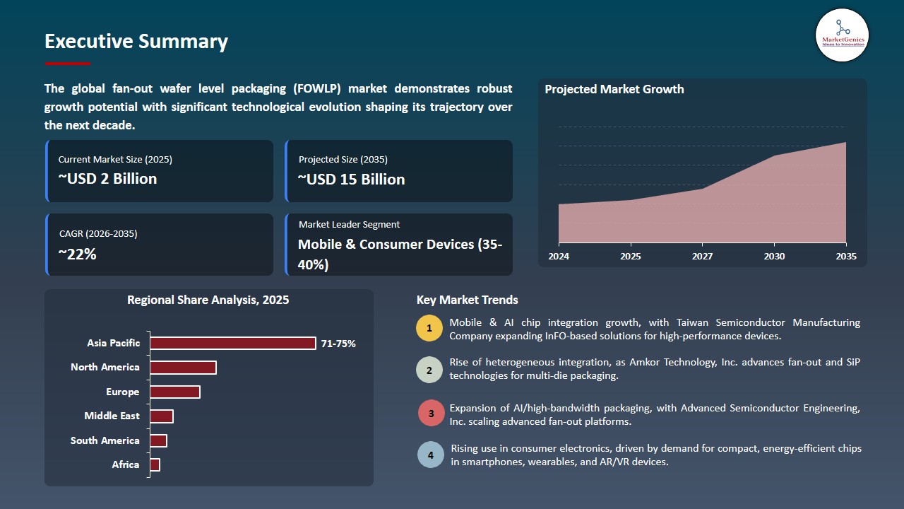
The global fan-out wafer level packaging (FOWLP) market is witnessing strong growth, valued at USD 2.1 billion in 2025 and projected to reach USD 14.8 billion by 2035, expanding at a CAGR of 21.6% during the forecast period. Advanced packaging technologies offer the potential to provide more functionality, higher data transfer rates, and greater power efficiency in shrinking electronic devices, making the fan-out wafer level packaging (FOWLP) market a high-density semiconductor integration system.
Young Liu, Chairman of Foxconn, remarked: This is not just a factory. It is a strategic platform for advanced manufacturing, semiconductor resilience, and future technologies in Europe. This project also supports Foxconn’s strategy of Build-Operate-Localize, which expands our global technology footprint through trusted partnerships.
Semiconductor packaging methods are changing the design and application of next-generation chips, and the global FOWLP market is emerging as a major contributor to the design of high-performance electronic systems. With the growing specialization of computing architectures, FOWLP creates faster signal propagation, enhanced energy efficiency, and increased functional density for AI accelerators, high-performance processors, automotive electronics, and high-speed communication systems.
The digital convergence of AI processors, advanced memory, and high-performance computing is being enabled by the increasing emphasis on next-generation packaging architectures that offers semiconductor design flexibility. In June 2026, Amkor highlighted its next-generation packaging platforms for AI, high-performance computing, photonics, and advanced memory applications, while strengthening collaborations with ecosystem leaders including AMD, Apple, NVIDIA, and TSMC to support increasingly complex semiconductor integration requirements.
Adjacent opportunity is the increasing shift to package-centric semiconductor architectures in which advanced packaging is increasingly a differentiator for system performance. FOWLP provides several functional components in a small area, with increased bandwidth and reduced power usage. Fan-out packaging has become a popular choice among manufacturers to meet the growing demand for scalable, flexible, and efficient applications in the fields of AI, edge computing, and high-performance networking.
Fan-Out Wafer Level Packaging (FOWLP) Market Dynamics and Trends
Driver: Rising Demand for AI, High-Performance Computing, and Advanced Mobile Processors
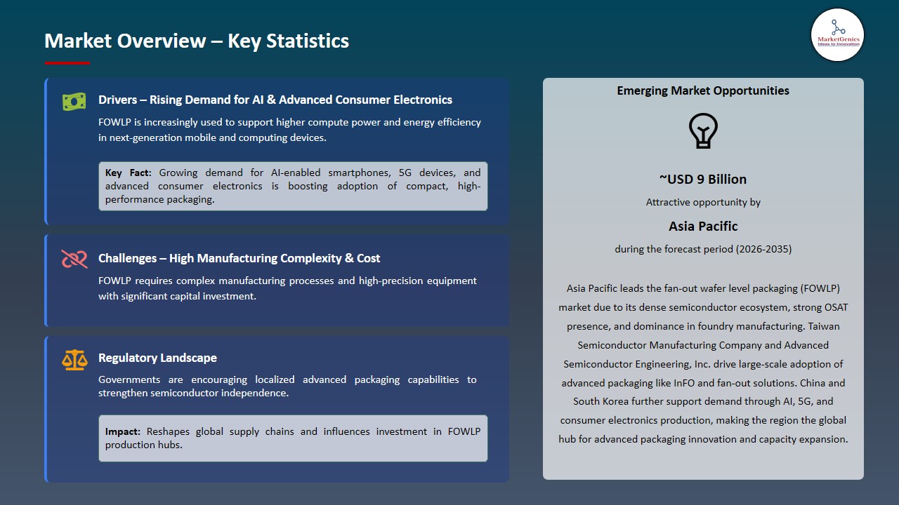
- The global fan-out wafer level packaging market is gaining significant momentum due to the need for higher bandwidth, integration density, and power efficiency in AI accelerators, high-performance computing systems, and advanced mobile processors to handle the rising demand for data-heavy workloads.
- As AI-powered computing platforms increasingly demand higher performance, semiconductor companies are pushing packaging innovation forward. For instance, in May 2026, Applied Materials announced its EPIC innovation partnership with Broadcom to accelerate development of new packaging technologies for advanced chips to enable higher interconnect density, heterogeneous integration and energy-efficient computing architectures in next-generation AI systems.
- The increasing adoption of AI infrastructure, sophisticated mobile devices and high-performance processors is driving demand across the globe for sophisticated FOWLP solutions.
Restraint: High Manufacturing Complexity and Production Costs
- The complexity of manufacturing fan-out wafer level packaging (FOWLP) with advanced redistribution layers (RDLs), heterogeneous integration, and chiplet designs is rising and presents a cost challenge for large-scale production.
- The package size and integration density keep expanding, advanced FOWLP processes impose strict requirements for the precision of wafer reconstitution, fine-line RDL fabrication, mold compound control, and warpage management during production, which introduces more risks for yield loss and process variation.
- Advanced FOWLP solutions are having a significant effect on large-scale global commercialization, due to increased equipment investment, process development expenses, and yield optimization needs.
Opportunity: Expansion of Chiplet-Based Architectures and Heterogeneous Integration
- The increasing application of chiplet based architecture and heterogeneous integration is likely to drive the global fan-out wafer level packaging market as it allows for significant performance, power efficiency and design flexibility gains for applications such as AI, data center and high performance computing.
- Collaborative chiplet ecosystems are being formed by industry players to spur the adoption of multi-die integration and advanced packaging. In January 2026, Cadence presented its Chiplet Spec-to-Packaged Parts ecosystem with Samsung Foundry, Arm and several IP partners, delivering pre-validated chiplet solutions that simplify the heterogeneous integration and speed the delivery of AI, data center, and high-performance computing applications.
- Advanced FOWLP solutions are seeing tremendous growth opportunities across the globe with the emergence of chiplet ecosystems and heterogeneous integration technologies.
Key Trend: Emergence of Panel-Level Fan-Out Packaging (FOPLP)
- The fan-out wafer level packaging (FOWLP) market is seeing a rising trend shifting toward panel-level fan-out packaging (FOPLP) to enhance manufacturing efficiency, package scalability, and throughput for AI, HPC, networking, and chiplet based semiconductor applications.
- The advanced packaging providers are trying to capitalize on the limitations of traditional wafer-based packaging by increasing panel production rates. For instance, in May 2026, ASE introduced a new first-of-its-kind, automated packaging production line compatible with its FOCoS and FOCoS-Bridge fan-out platforms, which can be used for AI, HPC, chiplet and high bandwidth memory applications.
- The combination of panel-level manufacturing, heterogeneous integration, and advanced chiplet architectures are driving the commercialization of FOPLP for next-generation semiconductor markets globally.
Fan-Out Wafer Level Packaging (FOWLP) Market Analysis and Segmental Data
Mobile & Consumer Devices Dominate Global Fan-Out Wafer Level Packaging (FOWLP) Market
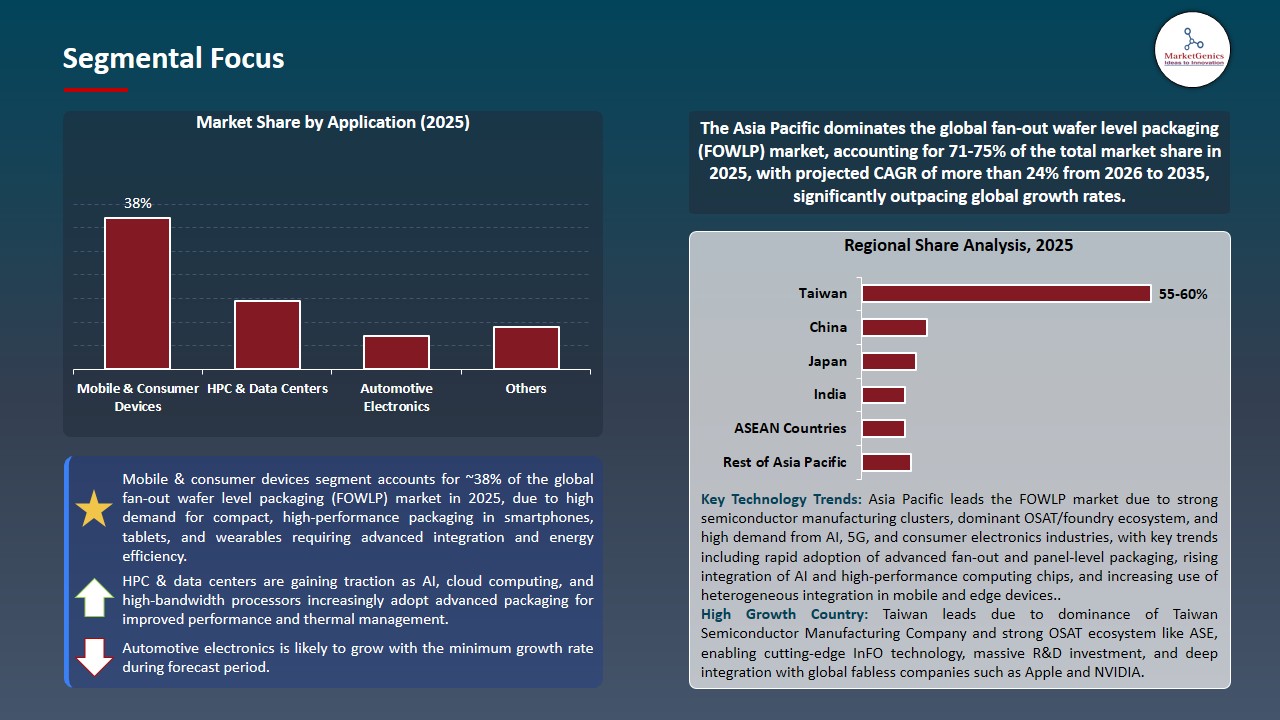
- Mobile & consumer devices dominates global fan-out wafer level packaging (FOWLP) market due to the higher compute density, and increased power efficiency continues to grow, advanced consumer electronics are increasingly pushing for compact and high performance semiconductor packaging solutions.
- Advanced packaging companies are making rapid strides in developments, aimed at the growing demand for high-performance mobile and consumer devices. In October 2024, Taiwan Semiconductor Manufacturing Company (TSMC) and Amkor Technology (ATK) announced another joint Integrated Fan-Out (InFO) initiative to boost their wafer-level packaging capability for high-end mobile processors and AI-powered consumer gadgets.
- AI smartphone, AR/VR devices, and advanced consumer electronics are driving the increasing adoption of FOWLP, which is projected to the steady growth.
Asia Pacific Leads Global Fan-Out Wafer Level Packaging (FOWLP) Market Demand
- The Asia Pacific leads the fan-out wafer level packaging market due to its robust semiconductor manufacturing industry, high number of OSAT vendors, increased AI chip production and rising adoption of advanced packaging technologies in Taiwan, South Korea, China, and Southeast Asia.
- Regional SEM leaders are pushing for next-gen packaging technologies to meet the increasing needs for AI and high performance computing. For instance, in April 2026, TSMC pushed forward its Chip-on-Panel-on-Substrate (CoPoS) roadmap, with the pilot line for the packaging process on panels coming to completion soon, showing that Asia Pacific is leading the way on the scalable fan-out and panel-based packaging architectures for next-generation AI processors.
- The growth of leading semiconductor foundries, advanced packaging companies, and expanding AI infrastructure further solidifies the Asia Pacific's leadership in the global wafer level packaging market.
Fan-Out Wafer Level Packaging (FOWLP) Market Ecosystem
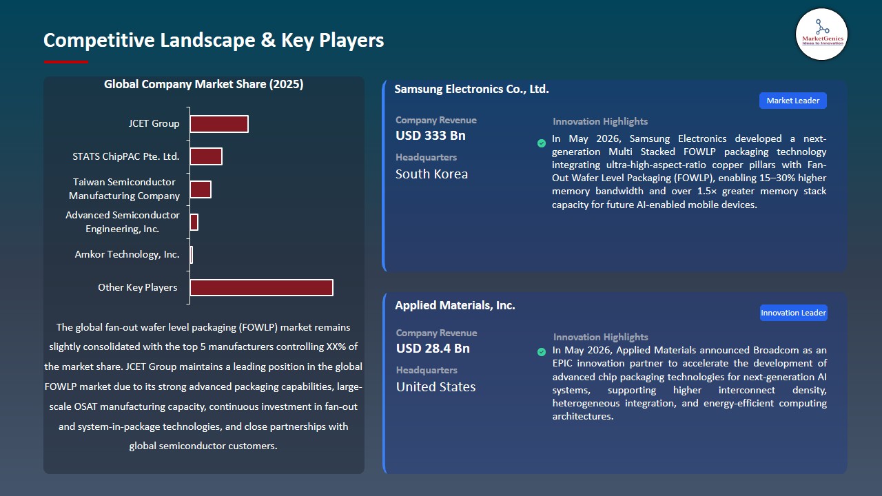
The fan-out wafer level packaging (FOWLP) market is moderately consolidated and is rapidly changing in terms of technology due to the advancements in semiconductor miniaturization, the growing demand for advanced high-performance and low-power chips for AI, automotive electronics, high-end mobile computing, and heterogeneous integration. Higher interconnect density and improved thermal performance and electrical efficiency are increasingly the result of the convergence of advanced packaging technologies, system-in-package (SiP) integration, and wafer-level process innovation.
JCET Group, STATS ChipPAC Pte. are some of the competitive players in the market., Taiwan Semiconductor Manufacturing Company (TSMC), Advanced Semiconductor Engineering, Inc. (ASE), and Amkor Technology, Inc. (Akor) are all aggressively developing advanced packaging technologies, including FOWLP, fan-out, and heterogeneous integration technologies. These are the companies that are developing advanced packaging ecosystems on a wafer level, with 2.5D/3D integration, substrate-less architecture, and AI chip packaging design.
The ecosystem is becoming more collaborative, with foundries, outsourced semiconductor assembly and test (OSAT) providers and the chip designers working more closely together, with more focus on chiplet-based architectures, system-level integration and co-design approaches. The global FOWLP market is increasingly becoming competitive, with the integration of the entire ecosystem, alignment with the supply chain, and innovative packaging solutions becoming key drivers.
 Recent Development and Strategic Overview
- In May 2026, Samsung Electronics announced the development of next-generation Multi Stacked FOWLP packaging technology that includes ultra-high-aspect-ratio copper pillars to provide 15–30% more memory bandwidth and more than 1.5× memory stack capacity for future AI-powered mobile devices.
- In May 2025, Foxconn joined Thales and Radiall to open Europe's first fan-out wafer level packaging (FOWLP) OSAT plant in France, bringing full packaging skills to support automotive, aerospace and defense, and 6G applications.
Report Scope
|
Detail |
|
|
Market Size in 2025 |
USD 2.1 Bn |
|
Market Forecast Value in 2035 |
USD 14.8 Bn |
|
Growth Rate (CAGR) |
21.6% |
|
Forecast Period |
2026 – 2035 |
|
Historical Data Available for |
2021 – 2024 |
|
Market Size Units |
US$ Billion for Value |
|
Report Format |
Electronic (PDF) + Excel |
|
North America |
Europe |
Asia Pacific |
Middle East |
Africa |
South America |
|
|
|
|
|
|
|
Companies Covered |
|||||
|
|||||
Fan-Out Wafer Level Packaging (FOWLP) Market Segmentation and Highlights
|
Segment |
Sub-segment |
|
Fan-Out Wafer Level Packaging (FOWLP) Market, By Packaging Technology |
|
|
Fan-Out Wafer Level Packaging (FOWLP) Market, By Carrier Type |
|
|
Fan-Out Wafer Level Packaging (FOWLP) Market, By Number of I/O Pins |
|
|
Fan-Out Wafer Level Packaging (FOWLP) Market, By Technology Node |
|
|
Fan-Out Wafer Level Packaging (FOWLP) Market, By Wafer Size |
|
|
Fan-Out Wafer Level Packaging (FOWLP) Market, By Integration Level |
|
|
Fan-Out Wafer Level Packaging (FOWLP) Market, By Application |
|
|
Fan-Out Wafer Level Packaging (FOWLP) Market, By End Users |
|
Frequently Asked Questions
Table of Contents
- 1. Research Methodology and Assumptions
- 1.1. Definitions
- 1.2. Research Design and Approach
- 1.3. Data Collection Methods
- 1.4. Base Estimates and Calculations
- 1.5. Forecasting Models
- 1.5.1. Key Forecast Factors & Impact Analysis
- 1.6. Secondary Research
- 1.6.1. Open Sources
- 1.6.2. Paid Databases
- 1.6.3. Associations
- 1.7. Primary Research
- 1.7.1. Primary Sources
- 1.7.2. Primary Interviews with Stakeholders across Ecosystem
- 2. Executive Summary
- 2.1. Global Fan-Out Wafer Level Packaging (FOWLP) Market Outlook
- 2.1.1. Fan-Out Wafer Level Packaging (FOWLP) Market Size (Value - US$ Bn), and Forecasts, 2021-2035
- 2.1.2. Compounded Annual Growth Rate Analysis
- 2.1.3. Growth Opportunity Analysis
- 2.1.4. Segmental Share Analysis
- 2.1.5. Geographical Share Analysis
- 2.2. Market Analysis and Facts
- 2.3. Supply-Demand Analysis
- 2.4. Competitive Benchmarking
- 2.5. Go-to- Market Strategy
- 2.5.1. Customer/ End-use Industry Assessment
- 2.5.2. Growth Opportunity Data, 2026-2035
- 2.5.2.1. Regional Data
- 2.5.2.2. Country Data
- 2.5.2.3. Segmental Data
- 2.5.3. Identification of Potential Market Spaces
- 2.5.4. GAP Analysis
- 2.5.5. Potential Attractive Price Points
- 2.5.6. Prevailing Market Risks & Challenges
- 2.5.7. Preferred Sales & Marketing Strategies
- 2.5.8. Key Recommendations and Analysis
- 2.5.9. A Way Forward
- 2.1. Global Fan-Out Wafer Level Packaging (FOWLP) Market Outlook
- 3. Industry Data and Premium Insights
- 3.1. Global Semiconductor & Electronics Industry Overview, 2025
- 3.1.1. Semiconductor & Electronics Industry Ecosystem Analysis
- 3.1.2. Key Trends for Semiconductor & Electronics Industry
- 3.1.3. Regional Distribution for Semiconductor & Electronics Industry
- 3.2. Supplier Customer Data
- 3.3. Technology Roadmap and Developments
- 3.4. Trade Analysis
- 3.4.1. Import & Export Analysis, 2025
- 3.4.2. Top Importing Countries
- 3.4.3. Top Exporting Countries
- 3.5. Trump Tariff Impact Analysis
- 3.5.1. Manufacturer
- 3.5.1.1. Based on the component & Raw material
- 3.5.2. Supply Chain
- 3.5.3. End Consumer
- 3.5.1. Manufacturer
- 3.6. Raw Material Analysis
- 3.1. Global Semiconductor & Electronics Industry Overview, 2025
- 4. Market Overview
- 4.1. Market Dynamics
- 4.1.1. Drivers
- 4.1.1.1. Rising adoption of AI-enabled smartphones, tablets, and premium consumer electronics requiring high-performance, compact packaging
- 4.1.1.2. Growing demand for advanced heterogeneous integration and higher interconnect density in semiconductor devices
- 4.1.1.3. Expansion of 5G/6G, edge computing, and high-bandwidth applications increasing need for efficient chip packaging solutions
- 4.1.2. Restraints
- 4.1.2.1. High manufacturing cost and complex process integration of fan-out wafer-level packaging technologies
- 4.1.2.2. Yield challenges and technical limitations in scaling advanced packaging for mass production
- 4.1.1. Drivers
- 4.2. Key Trend Analysis
- 4.3. Regulatory Framework
- 4.3.1. Key Regulations, Norms, and Subsidies, by Key Countries
- 4.3.2. Tariffs and Standards
- 4.3.3. Impact Analysis of Regulations on the Market
- 4.4. Ecosystem Analysis
- 4.5. Porter’s Five Forces Analysis
- 4.6. PESTEL Analysis
- 4.7. Global Fan-Out Wafer Level Packaging (FOWLP) Market Demand
- 4.7.1. Historical Market Size – Value (US$ Bn), 2020-2024
- 4.7.2. Current and Future Market Size – Value (US$ Bn), 2026–2035
- 4.7.2.1. Y-o-Y Growth Trends
- 4.7.2.2. Absolute $ Opportunity Assessment
- 4.1. Market Dynamics
- 5. Competition Landscape
- 5.1. Competition structure
- 5.1.1. Fragmented v/s consolidated
- 5.2. Company Share Analysis, 2025
- 5.2.1. Global Company Market Share
- 5.2.2. By Region
- 5.2.2.1. North America
- 5.2.2.2. Europe
- 5.2.2.3. Asia Pacific
- 5.2.2.4. Middle East
- 5.2.2.5. Africa
- 5.2.2.6. South America
- 5.3. Product Comparison Matrix
- 5.3.1. Specifications
- 5.3.2. Market Positioning
- 5.3.3. Pricing
- 5.1. Competition structure
- 6. Global Fan-Out Wafer Level Packaging (FOWLP) Market Analysis, by Packaging Technology
- 6.1. Key Segment Analysis
- 6.2. Fan-Out Wafer Level Packaging (FOWLP) Market Size (Value - US$ Bn), Analysis, and Forecasts, by Packaging Technology, 2021-2035
- 6.2.1. Chip-First FOWLP
- 6.2.1.1. Face-Down Chip-First
- 6.2.1.2. Face-Up Chip-First
- 6.2.2. Chip-Last FOWLP
- 6.2.2.1. Redistribution Layer (RDL)-First
- 6.2.2.2. Mold-First Process
- 6.2.3. Embedded Die Fan-Out Packaging
- 6.2.4. Integrated Fan-Out Packaging
- 6.2.5. Hybrid Fan-Out Packaging
- 6.2.1. Chip-First FOWLP
- 7. Global Fan-Out Wafer Level Packaging (FOWLP) Market Analysis, by Carrier Type
- 7.1. Key Segment Analysis
- 7.2. Fan-Out Wafer Level Packaging (FOWLP) Market Size (Value - US$ Bn), Analysis, and Forecasts, by Carrier Type, 2021-2035
- 7.2.1. Wafer-Based FOWLP
- 7.2.2. Panel-Based FOWLP
- 7.2.3. Glass Carrier-Based Packaging
- 7.2.4. Silicon Interposer-Based Fan-Out
- 8. Global Fan-Out Wafer Level Packaging (FOWLP) Market Analysis, by Number of I/O Pins
- 8.1. Key Segment Analysis
- 8.2. Fan-Out Wafer Level Packaging (FOWLP) Market Size (Value - US$ Bn), Analysis, and Forecasts, by Number of I/O Pins, 2021-2035
- 8.2.1. Below 200 Pins
- 8.2.2. 200 – 500 Pins
- 8.2.3. 500 – 1,000 Pins
- 8.2.4. Above 1,000 Pins
- 9. Global Fan-Out Wafer Level Packaging (FOWLP) Market Analysis, by Technology Node
- 9.1. Key Segment Analysis
- 9.2. Fan-Out Wafer Level Packaging (FOWLP) Market Size (Value - US$ Bn), Analysis, and Forecasts, by Technology Node, 2021-2035
- 9.2.1. Below 7 nm
- 9.2.2. 7 nm – 10 nm
- 9.2.3. 10 nm – 28 nm
- 9.2.4. 28 nm – 65 nm
- 9.2.5. Above 65 nm
- 10. Global Fan-Out Wafer Level Packaging (FOWLP) Market Analysis, by Wafer Size
- 10.1. Key Segment Analysis
- 10.2. Fan-Out Wafer Level Packaging (FOWLP) Market Size (Value - US$ Bn), Analysis, and Forecasts, by Wafer Size, 2021-2035
- 10.2.1. Up to 200 mm
- 10.2.2. 300 mm
- 10.2.3. Above 300 mm
- 11. Global Fan-Out Wafer Level Packaging (FOWLP) Market Analysis, by Integration Level
- 11.1. Key Segment Analysis
- 11.2. Fan-Out Wafer Level Packaging (FOWLP) Market Size (Value - US$ Bn), Analysis, and Forecasts, by Integration Level, 2021-2035
- 11.2.1. Single Die Fan-Out
- 11.2.2. Multi-Die Fan-Out
- 11.2.3. Heterogeneous Integration
- 11.2.3.1. 2D Integration
- 11.2.3.2. 5D Integration
- 11.2.3.3. 3D Stacked Integration
- 11.2.4. Chiplet-Based Fan-Out Packaging
- 12. Global Fan-Out Wafer Level Packaging (FOWLP) Market Analysis, by Application
- 12.1. Key Segment Analysis
- 12.2. Fan-Out Wafer Level Packaging (FOWLP) Market Size (Value - US$ Bn), Analysis, and Forecasts, by Application, 2021-2035
- 12.2.1. Mobile & Consumer Devices
- 12.2.1.1. Mobile Application Processors
- 12.2.1.2. Wearable Electronics
- 12.2.1.3. AR/VR Processors
- 12.2.1.4. Others
- 12.2.2. Automotive Electronics
- 12.2.2.1. Advanced Driver Assistance Systems (ADAS)
- 12.2.2.2. In-Vehicle Infotainment (IVI)
- 12.2.2.3. Powertrain Control Modules
- 12.2.2.4. V2X Communication Modules
- 12.2.2.5. LiDAR & Radar Systems
- 12.2.2.6. Others
- 12.2.3. HPC & Data Centers
- 12.2.3.1. CPUs & GPUs
- 12.2.3.2. AI / ML Accelerators
- 12.2.3.3. Network Processors
- 12.2.3.4. Memory Interface Controllers
- 12.2.3.5. Others
- 12.2.4. Internet of Things (IoT) & Embedded Systems
- 12.2.5. Telecommunications & Networking
- 12.2.6. Medical & Healthcare Electronics
- 12.2.7. Industrial Electronics
- 12.2.8. Other Applications
- 12.2.1. Mobile & Consumer Devices
- 13. Global Fan-Out Wafer Level Packaging (FOWLP) Market Analysis, by End Users
- 13.1. Key Segment Analysis
- 13.2. Fan-Out Wafer Level Packaging (FOWLP) Market Size (Value - US$ Bn), Analysis, and Forecasts, by End Users, 2021-2035
- 13.2.1. Original Equipment Manufacturers
- 13.2.2. Integrated Device Manufacturers
- 13.2.3. Fabless Semiconductor Companies
- 13.2.4. OSAT Providers
- 13.2.5. Contract Electronics Manufacturers
- 13.2.6. Others
- 14. Global Fan-Out Wafer Level Packaging (FOWLP) Market Analysis and Forecasts, by Region
- 14.1. Key Findings
- 14.2. Fan-Out Wafer Level Packaging (FOWLP) Market Size (Value - US$ Bn), Analysis, and Forecasts, by Region, 2021-2035
- 14.2.1. North America
- 14.2.2. Europe
- 14.2.3. Asia Pacific
- 14.2.4. Middle East
- 14.2.5. Africa
- 14.2.6. South America
- 15. North America Fan-Out Wafer Level Packaging (FOWLP) Market Analysis
- 15.1. Key Segment Analysis
- 15.2. Regional Snapshot
- 15.3. North America Fan-Out Wafer Level Packaging (FOWLP) Market Size (Value - US$ Bn), Analysis, and Forecasts, 2021-2035
- 15.3.1. Packaging Technology
- 15.3.2. Carrier Type
- 15.3.3. Number of I/O Pins
- 15.3.4. Technology Node
- 15.3.5. Wafer Size
- 15.3.6. Integration Level
- 15.3.7. Application
- 15.3.8. End Users
- 15.3.9. Country
- 15.3.9.1. USA
- 15.3.9.2. Canada
- 15.3.9.3. Mexico
- 15.4. USA Fan-Out Wafer Level Packaging (FOWLP) Market
- 15.4.1. Country Segmental Analysis
- 15.4.2. Packaging Technology
- 15.4.3. Carrier Type
- 15.4.4. Number of I/O Pins
- 15.4.5. Technology Node
- 15.4.6. Wafer Size
- 15.4.7. Integration Level
- 15.4.8. Application
- 15.4.9. End Users
- 15.5. Canada Fan-Out Wafer Level Packaging (FOWLP) Market
- 15.5.1. Country Segmental Analysis
- 15.5.2. Packaging Technology
- 15.5.3. Carrier Type
- 15.5.4. Number of I/O Pins
- 15.5.5. Technology Node
- 15.5.6. Wafer Size
- 15.5.7. Integration Level
- 15.5.8. Application
- 15.5.9. End Users
- 15.6. Mexico Fan-Out Wafer Level Packaging (FOWLP) Market
- 15.6.1. Country Segmental Analysis
- 15.6.2. Packaging Technology
- 15.6.3. Carrier Type
- 15.6.4. Number of I/O Pins
- 15.6.5. Technology Node
- 15.6.6. Wafer Size
- 15.6.7. Integration Level
- 15.6.8. Application
- 15.6.9. End Users
- 16. Europe Fan-Out Wafer Level Packaging (FOWLP) Market Analysis
- 16.1. Key Segment Analysis
- 16.2. Regional Snapshot
- 16.3. Europe Fan-Out Wafer Level Packaging (FOWLP) Market Size (Value - US$ Bn), Analysis, and Forecasts, 2021-2035
- 16.3.1. Packaging Technology
- 16.3.2. Carrier Type
- 16.3.3. Number of I/O Pins
- 16.3.4. Technology Node
- 16.3.5. Wafer Size
- 16.3.6. Integration Level
- 16.3.7. Application
- 16.3.8. End Users
- 16.3.9. Country
- 16.3.9.1. Germany
- 16.3.9.2. United Kingdom
- 16.3.9.3. France
- 16.3.9.4. Italy
- 16.3.9.5. Spain
- 16.3.9.6. Netherlands
- 16.3.9.7. Nordic Countries
- 16.3.9.8. Poland
- 16.3.9.9. Russia & CIS
- 16.3.9.10. Rest of Europe
- 16.4. Germany Fan-Out Wafer Level Packaging (FOWLP) Market
- 16.4.1. Country Segmental Analysis
- 16.4.2. Packaging Technology
- 16.4.3. Carrier Type
- 16.4.4. Number of I/O Pins
- 16.4.5. Technology Node
- 16.4.6. Wafer Size
- 16.4.7. Integration Level
- 16.4.8. Application
- 16.4.9. End Users
- 16.5. United Kingdom Fan-Out Wafer Level Packaging (FOWLP) Market
- 16.5.1. Country Segmental Analysis
- 16.5.2. Packaging Technology
- 16.5.3. Carrier Type
- 16.5.4. Number of I/O Pins
- 16.5.5. Technology Node
- 16.5.6. Wafer Size
- 16.5.7. Integration Level
- 16.5.8. Application
- 16.5.9. End Users
- 16.6. France Fan-Out Wafer Level Packaging (FOWLP) Market
- 16.6.1. Country Segmental Analysis
- 16.6.2. Packaging Technology
- 16.6.3. Carrier Type
- 16.6.4. Number of I/O Pins
- 16.6.5. Technology Node
- 16.6.6. Wafer Size
- 16.6.7. Integration Level
- 16.6.8. Application
- 16.6.9. End Users
- 16.7. Italy Fan-Out Wafer Level Packaging (FOWLP) Market
- 16.7.1. Country Segmental Analysis
- 16.7.2. Packaging Technology
- 16.7.3. Carrier Type
- 16.7.4. Number of I/O Pins
- 16.7.5. Technology Node
- 16.7.6. Wafer Size
- 16.7.7. Integration Level
- 16.7.8. Application
- 16.7.9. End Users
- 16.8. Spain Fan-Out Wafer Level Packaging (FOWLP) Market
- 16.8.1. Country Segmental Analysis
- 16.8.2. Packaging Technology
- 16.8.3. Carrier Type
- 16.8.4. Number of I/O Pins
- 16.8.5. Technology Node
- 16.8.6. Wafer Size
- 16.8.7. Integration Level
- 16.8.8. Application
- 16.8.9. End Users
- 16.9. Netherlands Fan-Out Wafer Level Packaging (FOWLP) Market
- 16.9.1. Country Segmental Analysis
- 16.9.2. Packaging Technology
- 16.9.3. Carrier Type
- 16.9.4. Number of I/O Pins
- 16.9.5. Technology Node
- 16.9.6. Wafer Size
- 16.9.7. Integration Level
- 16.9.8. Application
- 16.9.9. End Users
- 16.10. Nordic Countries Fan-Out Wafer Level Packaging (FOWLP) Market
- 16.10.1. Country Segmental Analysis
- 16.10.2. Packaging Technology
- 16.10.3. Carrier Type
- 16.10.4. Number of I/O Pins
- 16.10.5. Technology Node
- 16.10.6. Wafer Size
- 16.10.7. Integration Level
- 16.10.8. Application
- 16.10.9. End Users
- 16.11. Poland Fan-Out Wafer Level Packaging (FOWLP) Market
- 16.11.1. Country Segmental Analysis
- 16.11.2. Packaging Technology
- 16.11.3. Carrier Type
- 16.11.4. Number of I/O Pins
- 16.11.5. Technology Node
- 16.11.6. Wafer Size
- 16.11.7. Integration Level
- 16.11.8. Application
- 16.11.9. End Users
- 16.12. Russia & CIS Fan-Out Wafer Level Packaging (FOWLP) Market
- 16.12.1. Country Segmental Analysis
- 16.12.2. Packaging Technology
- 16.12.3. Carrier Type
- 16.12.4. Number of I/O Pins
- 16.12.5. Technology Node
- 16.12.6. Wafer Size
- 16.12.7. Integration Level
- 16.12.8. Application
- 16.12.9. End Users
- 16.13. Rest of Europe Fan-Out Wafer Level Packaging (FOWLP) Market
- 16.13.1. Country Segmental Analysis
- 16.13.2. Packaging Technology
- 16.13.3. Carrier Type
- 16.13.4. Number of I/O Pins
- 16.13.5. Technology Node
- 16.13.6. Wafer Size
- 16.13.7. Integration Level
- 16.13.8. Application
- 16.13.9. End Users
- 17. Asia Pacific Fan-Out Wafer Level Packaging (FOWLP) Market Analysis
- 17.1. Key Segment Analysis
- 17.2. Regional Snapshot
- 17.3. Asia Pacific Fan-Out Wafer Level Packaging (FOWLP) Market Size (Value - US$ Bn), Analysis, and Forecasts, 2021-2035
- 17.3.1. Packaging Technology
- 17.3.2. Carrier Type
- 17.3.3. Number of I/O Pins
- 17.3.4. Technology Node
- 17.3.5. Wafer Size
- 17.3.6. Integration Level
- 17.3.7. Application
- 17.3.8. End Users
- 17.3.9. Country
- 17.3.9.1. China
- 17.3.9.2. India
- 17.3.9.3. Japan
- 17.3.9.4. South Korea
- 17.3.9.5. Australia and New Zealand
- 17.3.9.6. Indonesia
- 17.3.9.7. Malaysia
- 17.3.9.8. Thailand
- 17.3.9.9. Vietnam
- 17.3.9.10. Rest of Asia Pacific
- 17.4. China Fan-Out Wafer Level Packaging (FOWLP) Market
- 17.4.1. Country Segmental Analysis
- 17.4.2. Packaging Technology
- 17.4.3. Carrier Type
- 17.4.4. Number of I/O Pins
- 17.4.5. Technology Node
- 17.4.6. Wafer Size
- 17.4.7. Integration Level
- 17.4.8. Application
- 17.4.9. End Users
- 17.5. India Fan-Out Wafer Level Packaging (FOWLP) Market
- 17.5.1. Country Segmental Analysis
- 17.5.2. Packaging Technology
- 17.5.3. Carrier Type
- 17.5.4. Number of I/O Pins
- 17.5.5. Technology Node
- 17.5.6. Wafer Size
- 17.5.7. Integration Level
- 17.5.8. Application
- 17.5.9. End Users
- 17.6. Japan Fan-Out Wafer Level Packaging (FOWLP) Market
- 17.6.1. Country Segmental Analysis
- 17.6.2. Packaging Technology
- 17.6.3. Carrier Type
- 17.6.4. Number of I/O Pins
- 17.6.5. Technology Node
- 17.6.6. Wafer Size
- 17.6.7. Integration Level
- 17.6.8. Application
- 17.6.9. End Users
- 17.7. South Korea Fan-Out Wafer Level Packaging (FOWLP) Market
- 17.7.1. Country Segmental Analysis
- 17.7.2. Packaging Technology
- 17.7.3. Carrier Type
- 17.7.4. Number of I/O Pins
- 17.7.5. Technology Node
- 17.7.6. Wafer Size
- 17.7.7. Integration Level
- 17.7.8. Application
- 17.7.9. End Users
- 17.8. Australia and New Zealand Fan-Out Wafer Level Packaging (FOWLP) Market
- 17.8.1. Country Segmental Analysis
- 17.8.2. Packaging Technology
- 17.8.3. Carrier Type
- 17.8.4. Number of I/O Pins
- 17.8.5. Technology Node
- 17.8.6. Wafer Size
- 17.8.7. Integration Level
- 17.8.8. Application
- 17.8.9. End Users
- 17.9. Indonesia Fan-Out Wafer Level Packaging (FOWLP) Market
- 17.9.1. Country Segmental Analysis
- 17.9.2. Packaging Technology
- 17.9.3. Carrier Type
- 17.9.4. Number of I/O Pins
- 17.9.5. Technology Node
- 17.9.6. Wafer Size
- 17.9.7. Integration Level
- 17.9.8. Application
- 17.9.9. End Users
- 17.10. Malaysia Fan-Out Wafer Level Packaging (FOWLP) Market
- 17.10.1. Country Segmental Analysis
- 17.10.2. Packaging Technology
- 17.10.3. Carrier Type
- 17.10.4. Number of I/O Pins
- 17.10.5. Technology Node
- 17.10.6. Wafer Size
- 17.10.7. Integration Level
- 17.10.8. Application
- 17.10.9. End Users
- 17.11. Thailand Fan-Out Wafer Level Packaging (FOWLP) Market
- 17.11.1. Country Segmental Analysis
- 17.11.2. Packaging Technology
- 17.11.3. Carrier Type
- 17.11.4. Number of I/O Pins
- 17.11.5. Technology Node
- 17.11.6. Wafer Size
- 17.11.7. Integration Level
- 17.11.8. Application
- 17.11.9. End Users
- 17.12. Vietnam Fan-Out Wafer Level Packaging (FOWLP) Market
- 17.12.1. Country Segmental Analysis
- 17.12.2. Packaging Technology
- 17.12.3. Carrier Type
- 17.12.4. Number of I/O Pins
- 17.12.5. Technology Node
- 17.12.6. Wafer Size
- 17.12.7. Integration Level
- 17.12.8. Application
- 17.12.9. End Users
- 17.13. Rest of Asia Pacific Fan-Out Wafer Level Packaging (FOWLP) Market
- 17.13.1. Country Segmental Analysis
- 17.13.2. Packaging Technology
- 17.13.3. Carrier Type
- 17.13.4. Number of I/O Pins
- 17.13.5. Technology Node
- 17.13.6. Wafer Size
- 17.13.7. Integration Level
- 17.13.8. Application
- 17.13.9. End Users
- 18. Middle East Fan-Out Wafer Level Packaging (FOWLP) Market Analysis
- 18.1. Key Segment Analysis
- 18.2. Regional Snapshot
- 18.3. Middle East Fan-Out Wafer Level Packaging (FOWLP) Market Size (Value - US$ Bn), Analysis, and Forecasts, 2021-2035
- 18.3.1. Packaging Technology
- 18.3.2. Carrier Type
- 18.3.3. Number of I/O Pins
- 18.3.4. Technology Node
- 18.3.5. Wafer Size
- 18.3.6. Integration Level
- 18.3.7. Application
- 18.3.8. End Users
- 18.3.9. Country
- 18.3.9.1. Turkey
- 18.3.9.2. UAE
- 18.3.9.3. Saudi Arabia
- 18.3.9.4. Israel
- 18.3.9.5. Rest of Middle East
- 18.4. Turkey Fan-Out Wafer Level Packaging (FOWLP) Market
- 18.4.1. Country Segmental Analysis
- 18.4.2. Packaging Technology
- 18.4.3. Carrier Type
- 18.4.4. Number of I/O Pins
- 18.4.5. Technology Node
- 18.4.6. Wafer Size
- 18.4.7. Integration Level
- 18.4.8. Application
- 18.4.9. End Users
- 18.5. UAE Fan-Out Wafer Level Packaging (FOWLP) Market
- 18.5.1. Country Segmental Analysis
- 18.5.2. Packaging Technology
- 18.5.3. Carrier Type
- 18.5.4. Number of I/O Pins
- 18.5.5. Technology Node
- 18.5.6. Wafer Size
- 18.5.7. Integration Level
- 18.5.8. Application
- 18.5.9. End Users
- 18.6. Saudi Arabia Fan-Out Wafer Level Packaging (FOWLP) Market
- 18.6.1. Country Segmental Analysis
- 18.6.2. Packaging Technology
- 18.6.3. Carrier Type
- 18.6.4. Number of I/O Pins
- 18.6.5. Technology Node
- 18.6.6. Wafer Size
- 18.6.7. Integration Level
- 18.6.8. Application
- 18.6.9. End Users
- 18.7. Israel Fan-Out Wafer Level Packaging (FOWLP) Market
- 18.7.1. Country Segmental Analysis
- 18.7.2. Packaging Technology
- 18.7.3. Carrier Type
- 18.7.4. Number of I/O Pins
- 18.7.5. Technology Node
- 18.7.6. Wafer Size
- 18.7.7. Integration Level
- 18.7.8. Application
- 18.7.9. End Users
- 18.8. Rest of Middle East Fan-Out Wafer Level Packaging (FOWLP) Market
- 18.8.1. Country Segmental Analysis
- 18.8.2. Packaging Technology
- 18.8.3. Carrier Type
- 18.8.4. Number of I/O Pins
- 18.8.5. Technology Node
- 18.8.6. Wafer Size
- 18.8.7. Integration Level
- 18.8.8. Application
- 18.8.9. End Users
- 19. Africa Fan-Out Wafer Level Packaging (FOWLP) Market Analysis
- 19.1. Key Segment Analysis
- 19.2. Regional Snapshot
- 19.3. Africa Fan-Out Wafer Level Packaging (FOWLP) Market Size (Value - US$ Bn), Analysis, and Forecasts, 2021-2035
- 19.3.1. Packaging Technology
- 19.3.2. Carrier Type
- 19.3.3. Number of I/O Pins
- 19.3.4. Technology Node
- 19.3.5. Wafer Size
- 19.3.6. Integration Level
- 19.3.7. Application
- 19.3.8. End Users
- 19.3.9. Country
- 19.3.9.1. South Africa
- 19.3.9.2. Egypt
- 19.3.9.3. Nigeria
- 19.3.9.4. Algeria
- 19.3.9.5. Rest of Africa
- 19.4. South Africa Fan-Out Wafer Level Packaging (FOWLP) Market
- 19.4.1. Country Segmental Analysis
- 19.4.2. Packaging Technology
- 19.4.3. Carrier Type
- 19.4.4. Number of I/O Pins
- 19.4.5. Technology Node
- 19.4.6. Wafer Size
- 19.4.7. Integration Level
- 19.4.8. Application
- 19.4.9. End Users
- 19.5. Egypt Fan-Out Wafer Level Packaging (FOWLP) Market
- 19.5.1. Country Segmental Analysis
- 19.5.2. Packaging Technology
- 19.5.3. Carrier Type
- 19.5.4. Number of I/O Pins
- 19.5.5. Technology Node
- 19.5.6. Wafer Size
- 19.5.7. Integration Level
- 19.5.8. Application
- 19.5.9. End Users
- 19.6. Nigeria Fan-Out Wafer Level Packaging (FOWLP) Market
- 19.6.1. Country Segmental Analysis
- 19.6.2. Packaging Technology
- 19.6.3. Carrier Type
- 19.6.4. Number of I/O Pins
- 19.6.5. Technology Node
- 19.6.6. Wafer Size
- 19.6.7. Integration Level
- 19.6.8. Application
- 19.6.9. End Users
- 19.7. Algeria Fan-Out Wafer Level Packaging (FOWLP) Market
- 19.7.1. Country Segmental Analysis
- 19.7.2. Packaging Technology
- 19.7.3. Carrier Type
- 19.7.4. Number of I/O Pins
- 19.7.5. Technology Node
- 19.7.6. Wafer Size
- 19.7.7. Integration Level
- 19.7.8. Application
- 19.7.9. End Users
- 19.8. Rest of Africa Fan-Out Wafer Level Packaging (FOWLP) Market
- 19.8.1. Country Segmental Analysis
- 19.8.2. Packaging Technology
- 19.8.3. Carrier Type
- 19.8.4. Number of I/O Pins
- 19.8.5. Technology Node
- 19.8.6. Wafer Size
- 19.8.7. Integration Level
- 19.8.8. Application
- 19.8.9. End Users
- 20. South America Fan-Out Wafer Level Packaging (FOWLP) Market Analysis
- 20.1. Key Segment Analysis
- 20.2. Regional Snapshot
- 20.3. South America Fan-Out Wafer Level Packaging (FOWLP) Market Size (Value - US$ Bn), Analysis, and Forecasts, 2021-2035
- 20.3.1. Packaging Technology
- 20.3.2. Carrier Type
- 20.3.3. Number of I/O Pins
- 20.3.4. Technology Node
- 20.3.5. Wafer Size
- 20.3.6. Integration Level
- 20.3.7. Application
- 20.3.8. End Users
- 20.3.9. Country
- 20.3.9.1. Brazil
- 20.3.9.2. Argentina
- 20.3.9.3. Rest of South America
- 20.4. Brazil Fan-Out Wafer Level Packaging (FOWLP) Market
- 20.4.1. Country Segmental Analysis
- 20.4.2. Packaging Technology
- 20.4.3. Carrier Type
- 20.4.4. Number of I/O Pins
- 20.4.5. Technology Node
- 20.4.6. Wafer Size
- 20.4.7. Integration Level
- 20.4.8. Application
- 20.4.9. End Users
- 20.5. Argentina Fan-Out Wafer Level Packaging (FOWLP) Market
- 20.5.1. Country Segmental Analysis
- 20.5.2. Packaging Technology
- 20.5.3. Carrier Type
- 20.5.4. Number of I/O Pins
- 20.5.5. Technology Node
- 20.5.6. Wafer Size
- 20.5.7. Integration Level
- 20.5.8. Application
- 20.5.9. End Users
- 20.6. Rest of South America Fan-Out Wafer Level Packaging (FOWLP) Market
- 20.6.1. Country Segmental Analysis
- 20.6.2. Packaging Technology
- 20.6.3. Carrier Type
- 20.6.4. Number of I/O Pins
- 20.6.5. Technology Node
- 20.6.6. Wafer Size
- 20.6.7. Integration Level
- 20.6.8. Application
- 20.6.9. End Users
- 21. Key Players/ Company Profile
- 21.1. Advanced Semiconductor Engineering, Inc.
- 21.1.1. Company Details/ Overview
- 21.1.2. Company Financials
- 21.1.3. Key Customers and Competitors
- 21.1.4. Business/ Industry Portfolio
- 21.1.5. Product Portfolio/ Specification Details
- 21.1.6. Pricing Data
- 21.1.7. Strategic Overview
- 21.1.8. Recent Developments
- 21.2. Amkor Technology, Inc.
- 21.3. CHIPBOND Technology Corporation
- 21.4. Deca Technologies Inc.
- 21.5. Infineon Technologies AG
- 21.6. JCET Group
- 21.7. Nepes Corporation
- 21.8. Powertech Technology Inc.
- 21.9. Samsung Electronics Co., Ltd.
- 21.10. Siliconware Precision Industries Co., Ltd.
- 21.11. STATS ChipPAC Pte. Ltd.
- 21.12. Taiwan Semiconductor Manufacturing Company
- 21.13. Tianshui Huatian Technology Co Ltd
- 21.14. Tongfu Microelectronics Co., Ltd.
- 21.15. Other Key Players
- 21.1. Advanced Semiconductor Engineering, Inc.
Note* - This is just tentative list of players. While providing the report, we will cover more number of players based on their revenue and share for each geography
Research Design
Our research design integrates both demand-side and supply-side analysis through a balanced combination of primary and secondary research methodologies. By utilizing both bottom-up and top-down approaches alongside rigorous data triangulation methods, we deliver robust market intelligence that supports strategic decision-making.
MarketGenics' comprehensive research design framework ensures the delivery of accurate, reliable, and actionable market intelligence. Through the integration of multiple research approaches, rigorous validation processes, and expert analysis, we provide our clients with the insights needed to make informed strategic decisions and capitalize on market opportunities.
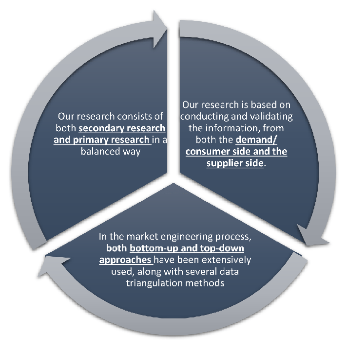
MarketGenics leverages a dedicated industry panel of experts and a comprehensive suite of paid databases to effectively collect, consolidate, and analyze market intelligence.
Our approach has consistently proven to be reliable and effective in generating accurate market insights, identifying key industry trends, and uncovering emerging business opportunities.
Through both primary and secondary research, we capture and analyze critical company-level data such as manufacturing footprints, including technical centers, R&D facilities, sales offices, and headquarters.
Our expert panel further enhances our ability to estimate market size for specific brands based on validated field-level intelligence.
Our data mining techniques incorporate both parametric and non-parametric methods, allowing for structured data collection, sorting, processing, and cleaning.
Demand projections are derived from large-scale data sets analyzed through proprietary algorithms, culminating in robust and reliable market sizing.
Research Approach
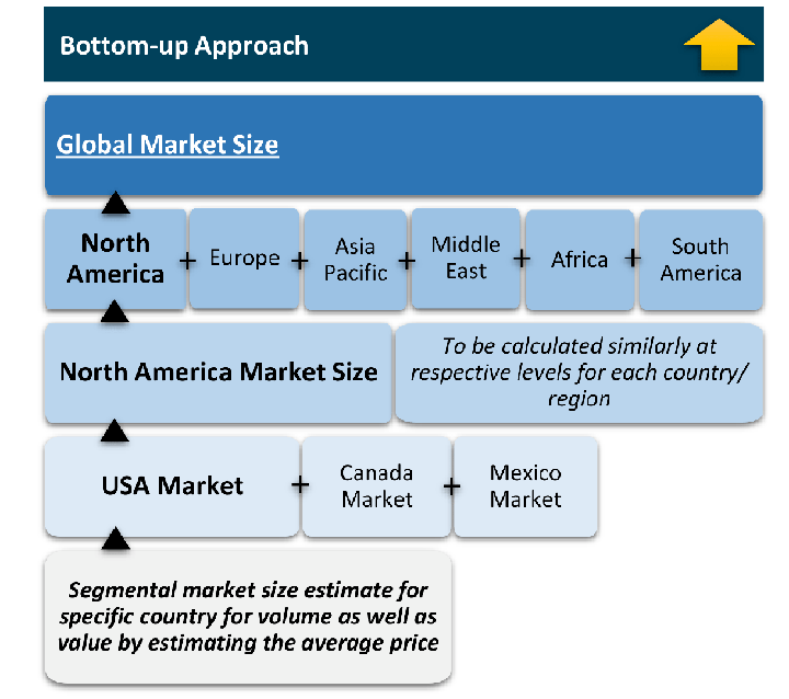
The bottom-up approach builds market estimates by starting with the smallest addressable market units and systematically aggregating them to create comprehensive market size projections.
This method begins with specific, granular data points and builds upward to create the complete market landscape.
Customer Analysis → Segmental Analysis → Geographical Analysis
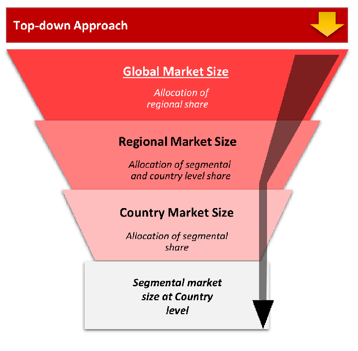
The top-down approach starts with the broadest possible market data and systematically narrows it down through a series of filters and assumptions to arrive at specific market segments or opportunities.
This method begins with the big picture and works downward to increasingly specific market slices.
TAM → SAM → SOM
Research Methods
Desk / Secondary Research
While analysing the market, we extensively study secondary sources, directories, and databases to identify and collect information useful for this technical, market-oriented, and commercial report. Secondary sources that we utilize are not only the public sources, but it is a combination of Open Source, Associations, Paid Databases, MG Repository & Knowledgebase, and others.
- Company websites, annual reports, financial reports, broker reports, and investor presentations
- National government documents, statistical databases and reports
- News articles, press releases and web-casts specific to the companies operating in the market, Magazines, reports, and others
- We gather information from commercial data sources for deriving company specific data such as segmental revenue, share for geography, product revenue, and others
- Internal and external proprietary databases (industry-specific), relevant patent, and regulatory databases
- Governing Bodies, Government Organizations
- Relevant Authorities, Country-specific Associations for Industries
We also employ the model mapping approach to estimate the product level market data through the players' product portfolio
Primary Research
Primary research/ interviews is vital in analyzing the market. Most of the cases involves paid primary interviews. Primary sources include primary interviews through e-mail interactions, telephonic interviews, surveys as well as face-to-face interviews with the different stakeholders across the value chain including several industry experts.
| Type of Respondents | Number of Primaries |
|---|---|
| Tier 2/3 Suppliers | ~20 |
| Tier 1 Suppliers | ~25 |
| End-users | ~25 |
| Industry Expert/ Panel/ Consultant | ~30 |
| Total | ~100 |
MG Knowledgebase
• Repository of industry blog, newsletter and case studies
• Online platform covering detailed market reports, and company profiles
Forecasting Factors and Models
Forecasting Factors
- Historical Trends – Past market patterns, cycles, and major events that shaped how markets behave over time. Understanding past trends helps predict future behavior.
- Industry Factors – Specific characteristics of the industry like structure, regulations, and innovation cycles that affect market dynamics.
- Macroeconomic Factors – Economic conditions like GDP growth, inflation, and employment rates that affect how much money people have to spend.
- Demographic Factors – Population characteristics like age, income, and location that determine who can buy your product.
- Technology Factors – How quickly people adopt new technology and how much technology infrastructure exists.
- Regulatory Factors – Government rules, laws, and policies that can help or restrict market growth.
- Competitive Factors – Analyzing competition structure such as degree of competition and bargaining power of buyers and suppliers.
Forecasting Models / Techniques
Multiple Regression Analysis
- Identify and quantify factors that drive market changes
- Statistical modeling to establish relationships between market drivers and outcomes
Time Series Analysis – Seasonal Patterns
- Understand regular cyclical patterns in market demand
- Advanced statistical techniques to separate trend, seasonal, and irregular components
Time Series Analysis – Trend Analysis
- Identify underlying market growth patterns and momentum
- Statistical analysis of historical data to project future trends
Expert Opinion – Expert Interviews
- Gather deep industry insights and contextual understanding
- In-depth interviews with key industry stakeholders
Multi-Scenario Development
- Prepare for uncertainty by modeling different possible futures
- Creating optimistic, pessimistic, and most likely scenarios
Time Series Analysis – Moving Averages
- Sophisticated forecasting for complex time series data
- Auto-regressive integrated moving average models with seasonal components
Econometric Models
- Apply economic theory to market forecasting
- Sophisticated economic models that account for market interactions
Expert Opinion – Delphi Method
- Harness collective wisdom of industry experts
- Structured, multi-round expert consultation process
Monte Carlo Simulation
- Quantify uncertainty and probability distributions
- Thousands of simulations with varying input parameters
Research Analysis
Our research framework is built upon the fundamental principle of validating market intelligence from both demand and supply perspectives. This dual-sided approach ensures comprehensive market understanding and reduces the risk of single-source bias.
Demand-Side Analysis: We understand end-user/application behavior, preferences, and market needs along with the penetration of the product for specific application.
Supply-Side Analysis: We estimate overall market revenue, analyze the segmental share along with industry capacity, competitive landscape, and market structure.
Validation & Evaluation
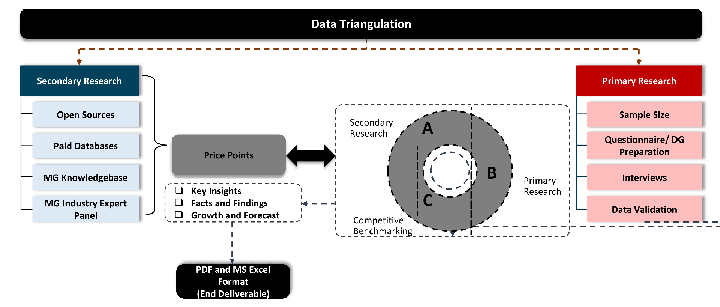
Data triangulation is a validation technique that uses multiple methods, sources, or perspectives to examine the same research question, thereby increasing the credibility and reliability of research findings. In market research, triangulation serves as a quality assurance mechanism that helps identify and minimize bias, validate assumptions, and ensure accuracy in market estimates.
- Data Source Triangulation – Using multiple data sources to examine the same phenomenon
- Methodological Triangulation – Using multiple research methods to study the same research question
- Investigator Triangulation – Using multiple researchers or analysts to examine the same data
- Theoretical Triangulation – Using multiple theoretical perspectives to interpret the same data
Custom Market Research Services
We will customise the research for you, in case the report listed above does not meet your requirements.
Get 10% Free Customisation